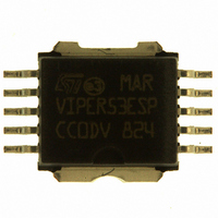
VIPER53ESPTR-E STMicroelectronics, VIPER53ESPTR-E Datasheet - Page 10

VIPER53ESPTR-E
Manufacturer Part Number
VIPER53ESPTR-E
Description
IC OFFLINE SWIT PWM POWERSO10
Manufacturer
STMicroelectronics
Series
VIPER™r
Datasheet
1.VIPER53ESPTR-E.pdf
(31 pages)
Specifications of VIPER53ESPTR-E
Output Isolation
Isolated
Frequency Range
93 ~ 300kHz
Voltage - Input
8.4 ~ 19 V
Voltage - Output
620V
Power (watts)
40W
Operating Temperature
25°C ~ 125°C
Package / Case
PowerSO-10 Exposed Bottom Pad
On Resistance (max)
1.7 Ohms
Supply Voltage (max)
19 V
Supply Voltage (min)
2.6 V
Maximum Operating Temperature
+ 150 C
Minimum Operating Temperature
- 40 C
Mounting Style
SMD/SMT
Number Of Switches
Single
Off Isolation (typ)
8.4 V
Operating Temperature (max)
150C
Operating Temperature (min)
-40C
Pin Count
10
Mounting
Surface Mount
Package Type
PowerSO
Screening Level
Automotive
For Use With
497-8435 - BOARD EVAL FOR VIPER53 28W497-6458 - BOARD EVAL BASED ON VIPER53-E497-6262 - BOARD REF SGL VIPER53 90-264VAC497-5866 - EVAL BOARD 24W NEG OUT VIPER53E497-5865 - EVAL BOARD 24W POS OUT VIPER53E497-4933 - BOARD PWR SUPPLY 24W OUTPUT VIPE
Lead Free Status / RoHS Status
Lead free / RoHS Compliant
Other names
497-5772-2
Available stocks
Company
Part Number
Manufacturer
Quantity
Price
Company:
Part Number:
VIPER53ESPTR-E
Manufacturer:
TI
Quantity:
1 500
Part Number:
VIPER53ESPTR-E
Manufacturer:
ST
Quantity:
20 000
Current Mode Topology
6
10/31
Current Mode Topology
The VIPer53E implements the conventional current mode control method for regulating the
output voltage. This kind of feedback includes two nested regulation loops:
The inner loop controls the peak primary current cycle by cycle. When the Power MOSFET
output transistor is on, the inductor current (primary side of the transformer) is monitored
with a SenseFET technique and converted into a voltage. When V
power switch is turned off. This structure is completely integrated as shown on the Block
Diagram of
time function and the PWM latch. The following formula gives the peak current in the Power
MOSFET according to the compensation voltage:
The outer loop defines the level at which the inner loop regulates peak current in the power
switch. For this purpose, V
optocoupler in secondary feedback configuration, see
accordingly the peak drain current for each switching cycle.
As the inner loop regulates the peak primary current in the primary side of the transformer,
all input voltage changes are compensated for before impacting the output voltage. This
results in an improved line regulation, instantaneous correction to line changes, and better
stability for the voltage regulation loop.
Current mode topology also provides a good converter start-up control. The compensation
voltage can be controlled to increase slowly during the start-up phase, so the peak primary
current will follow this soft voltage slope to provide a smooth output voltage rise, without any
overshoot. The simpler voltage mode structure which only controls the duty cycle, leads
generally to high current at start-up with the risk of transformer saturation.
An integrated blanking filter inhibits the PWM comparator output for a short time after the
integrated Power MOSFET is switched on. This function prevents anomalous or premature
termination of the switching pulse in the case of current spikes caused by primary side
transformer capacitance or secondary side rectifier reverse recovery time when working in
continuous mode.
Figure on page
COMP
1, with the current amplifier, the PWM comparator, the blanking
I
is driven by the feedback network (TL431 through an
Dpeak
DocRev1
=
V
------------------------------------------------- -
COMP
H
COMP
–
V
COMPos
Figure 3 on page
VIPer53EDIP - E / VIPer53ESP - E
S
reaches V
8) and is sets
COMP
, the


