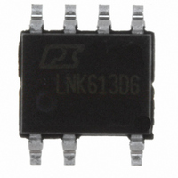
LNK613DG Power Integrations, LNK613DG Datasheet

LNK613DG
Specifications of LNK613DG
Available stocks
Related parts for LNK613DG
LNK613DG Summary of contents
Page 1
LNK603-606/613-616 LinkSwitch-II Family ® Energy-Efficient, Accurate CV/CC Switcher for Adapters and Chargers Product Highlights Dramatically Simplifies CV/CC Converters Eliminates optocoupler and all secondary CV/CC control circuitry • Eliminates all control loop compensation circuitry • Advanced Performance Features Compensates for transformer ...
Page 2
LNK603-606/613-616 BYPASS (BP/M) + FEEDBACK (FB) t SAMPLE-OUT CABLE DROP COMPENSATION 6.5 V INDUCTANCE CORRECTION SOURCE CONSTANT (S) CURRENT Figure 2 Functional Block Diagram. Pin Functional Description DRAIN (D) Pin: This pin is the power MOSFET drain ...
Page 3
LinkSwitch-II Functional Description The LinkSwitch-II combines a high voltage power MOSFET switch with a power supply controller in one device. Similar to the LinkSwitch-LP and TinySwitch-III it uses ON/OFF control to regulate the output voltage. In addition, the switching frequency ...
Page 4
... Energy Efficient USB Charger Power Supply (74% Average Efficiency, <30 mW No-load Input Power). Circuit Description This circuit shown in Figure 4 is configured as a primary-side regulated flyback power supply utilizing the LNK613DG. With an average efficiency of 74% and <30 mW no-load input power this design easily exceeds the most stringent current energy efficiency requirements ...
Page 5
The feedback resistors (R5 and R6) were selected using standard 1% resistor values to center both the nominal output voltage and constant current regulation thresholds. Key Application Considerations Output Power Table ...
Page 6
LNK603-606/613-616 Input Stage Feedback R2 Resistors Bypass Capacitor D3 RF1 AC Input Figure 5. PCB Layout Example Showing 5.1 W Design Using P Package. Secondary Loop Area To minimize leakage inductance and ...
Page 7
... C1 C2 4.7 µF 4.7 µF 400 V 400 V D5 1N4007 LinkSwitch-II U1 LNK613DG C4 1 µ former saturation and excessive leading edge current spikes. and V are provided in BP LinkSwitch-II has a leading edge blanking time of 170 ns to prevent premature termination of the ON-cycle. 3. Thermal check – At maximum output power, both minimum and maximum input voltage and maximum ambient tempera- ture ...
Page 8
LNK603-606/613-616 Absolute Maximum Ratings (1,4) DRAIN Voltage .................................. ......... ..............-0 700 V DRAIN Peak Current: LNK603/613 ...................320 (480) mA LNK604/614 .................. 400 (600) mA LNK605/615 .................. 504 (750) mA LNK606/616 .................. 654 (980) mA Peak Negative Pulsed Drain ...
Page 9
Parameter Symbol Control Functions (cont.) Cable Compensation υ Factor FB Switch ON-Time t ON Minimum Switch t ON-Time ON(min) FEEDBACK Pin t Sampling Delay DRAIN Supply Current CH1 BYPASS Pin Charge Current I CH2 ...
Page 10
LNK603-606/613-616 Parameter Symbol Output ON-State R Resistance DS(ON) I DSS1 OFF-State Leakage I DSS2 Breakdown BV Voltage DSS DRAIN Supply Voltage Auto-Restart t ON-Time AR-ON Auto-Restart t OFF-Time AR-OFF Open-Loop FEEDBACK Pin I OL Current Threshold Open-Loop ON-Time NOTES: 1. ...
Page 11
Typical Performance Characteristics 1.200 1.000 0.800 0.600 0.400 0.200 0.000 -40 - Temperature (°C) Figure 9. Current Limit vs. Temperature. 1.200 1.000 0.800 0.600 0.400 0.200 0.000 -40 - Temperature (°C) Figure 11. Frequency ...
Page 12
LNK603-606/613-616 Typical Performance Characteristics (cont.) 1.1 1.0 0.9 -50 - 100 125 150 Junction Temperature (°C) Figure 15. Breakdown vs. Temperature. 1000 100 Scaling Factors: LNK6X3 1.0 LNK6X4 1.0 LNK6X5 1.5 LNK6X6 2 ...
Page 13
Raise V voltage from 6.2 V, down Raise V until cycle skipping occurs Reduce V until cycle skipping stops at ...
Page 14
LNK603-606/613-616 470 pF 200 V 200 Ω µF 1)The transformer inductance is chosen to set the value chosen to operate test circuit in the CC region measured ...
Page 15
D S .004 (.10) -E- .240 (6.10) .260 (6.60) Pin 1 .367 (9.32) -D- .387 (9.83) .125 (3.18) .145 (3.68) -T- SEATING PLANE .100 (2.54) BSC .048 (1.22) .053 (1.35) .014 (.36) ⊕ .010 (.25) ...
Page 16
LNK603-606/613-616 B 4 4.90 (0.193) BSC A 8 3.90 (0.154) BSC 2 0.10 (0.004 Pin 1 ID 1.27 (0.050) BSC 1.25 - 1.65 1.35 (0.053) 1.75 (0.069) (0.049 - 0.065) 0.10 (0.004) 0.25 (0.010) Reference Solder ...
Page 17
LNK603-606/613-616 17 Rev. F 01/10 ...
Page 18
... The products and applications illustrated herein (including transformer construction and circuits external to the products) may be covered by one or more U.S. and foreign patents, or potentially by pending U.S. and foreign patent applications assigned to Power Integrations. A complete list of Power Integrations patents may be found at www.powerint.com. Power Integrations grants its customers a license under certain patent rights as set forth at http://www ...


