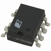
LNK520GN Power Integrations, LNK520GN Datasheet - Page 10

LNK520GN
Manufacturer Part Number
LNK520GN
Description
IC SWIT OCP CV/CC HV 8SMD
Manufacturer
Power Integrations
Series
LinkSwitch®r
Datasheet
1.LNK520PN.pdf
(20 pages)
Specifications of LNK520GN
Output Isolation
Isolated
Frequency Range
24 ~ 49.5kHz
Voltage - Output
700V
Power (watts)
5.50W
Operating Temperature
-40°C ~ 150°C
Package / Case
8-SMD Gull Wing, 7 Leads
Output Voltage
5.6 V
Input / Supply Voltage (max)
265 VAC
Input / Supply Voltage (min)
85 VAC
Duty Cycle (max)
80 %
Switching Frequency
42 KHz
Supply Current
0.75 mA
Operating Temperature Range
- 40 C to + 150 C
Mounting Style
SMD/SMT
For Use With
596-1006 - KIT DESIGN ACCELERATOR ADAPTER
Lead Free Status / RoHS Status
Lead free / RoHS Compliant
Available stocks
Company
Part Number
Manufacturer
Quantity
Price
Company:
Part Number:
LNK520GN
Manufacturer:
POWER
Quantity:
15 000
Part Number:
LNK520GN
Manufacturer:
POWER
Quantity:
20 000
Company:
Part Number:
LNK520GN-TL
Manufacturer:
ST
Quantity:
245
Company:
Part Number:
LNK520GN-TL
Manufacturer:
PowerInt
Quantity:
3 000
Part Number:
LNK520GN-TL
Manufacturer:
POWER
Quantity:
20 000
Feedback Resistor – R4
The value of R4 is selected to give a feedback current into the
CONTROL pin of approximately 2.15 mA at the peak output
power point of the supply. The actual value depends on the bias
voltage, typically in the range 20 V to 35 V, selected during
design. Higher values for the bias voltage will increase no-load
power consumption. Any 1%, 0.25 W resistor is suitable.
Output Diode – D7
PN fast, PN ultra-fast or Schottky diodes can be used depending
on the efficiency target for the supply, Schottky diodes giving
higher efficiency than PN diodes. The diode voltage rating
should be sufficient to withstand the output voltage plus the
input voltage transformed through the turns ratio (a typical V
of 50 V requires a diode PIV of 50 V). Slow recovery diodes
are not recommended (1N400X types).
Output Capacitor – C6
Capacitor C6 should be selected such that its voltage and
ripple current specifications are not exceeded. Selecting a
capacitor with low equivalent series resistance (ESR) will
reduce peak-peak output ripple and improve overall supply
operating efficiency.
LinkSwitch Layout considerations
Primary Side Connections
The copper area connected to SOURCE should be maximized
to minimize temperature rise of the LinkSwitch device.
The CONTROL pin capacitor C5 should be located as close as
possible to the SOURCE and CONTROL pins.
To minimize EMI coupling from the switching DRAIN node on
the primary to both the secondary and AC input, the LinkSwitch
should be positioned away from the secondary of the transformer
and AC input.
The length and copper area of all PCB traces connecting to the
switching DRAIN node should be kept to an absolute minimum
to limit EMI radiation.
Y capacitor
If a Y capacitor is required, it should be connected close to the
transformer secondary output return pin(s) and the primary bulk
capacitor positive terminal. Such placement will maximize the
EMI benefit of the Y capacitor and avoid problems in common-
mode surge testing.
10
LNK520
E
2/05
OR
Quick Design Checklist
As with any power supply design, all LinkSwitch designs
should be verified on the bench to make sure that component
specifications are not exceeded under worst-case conditions.
Performing the following minimum set of tests is strongly
recommended:
1. Maximum drain voltage – Verify that V
2. Maximum drain current – At maximum ambient temperature,
3. Thermal check – At peak output power, minimum input
4. Centered output characteristic – Using a transformer with
Selecting Between LNK500 and LNK520
The LNK500 and LNK520 differ in the circuit location of the
LinkSwitch device. The LNK500 is designed for high-side
operation and the LNK520 is designed for low-side operation.
The LNK520 can, however, be used in the high-side configuration
in certain applications. Refer to Figure 9 and supporting
description. Table 2 summarizes the considerations for selecting
which device to use.
Design Tools
Up to date information on design tools can be found at the
Power Integrations Web site: www.powerint.com.
675 V at highest input voltage and peak output power.
maximum input voltage and peak output power, verify drain
current waveforms at start-up for any signs of transformer
saturation and excessive leading edge current spikes.
LinkSwitch has a minimum leading edge blanking time of
200 ns to prevent premature termination of the on-cycle.
Verify that the leading edge current spike event is below
current limit at the end of the 200 ns blanking period.
voltage and maximum ambient temperature, verify that the
temperature specifications are not exceeded for LinkSwitch,
transformer, output diode and output capacitors. Enough
thermal margin should be allowed for part-to-part variation of
the R
low line, peak power, a maximum LinkSwitch SOURCE pin
temperature of 100 °C is recommended to allow for these
variations.
nominal primary inductance and at an input voltage midway
between low and high line, verify that the peak power point
occurs at ~4% above the desired nominal output current,
with the correct output voltage. If this does not occur, then
the design should be refined (increase L
overall tolerance limits are met.
DS(ON)
of LinkSwitch as specified in the data sheet. Under
DS
P
does not exceed
) to ensure the


