LNK306DN-TL Power Integrations, LNK306DN-TL Datasheet - Page 9
LNK306DN-TL
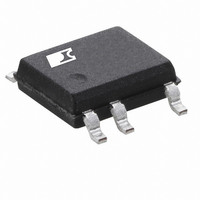
Manufacturer Part Number
LNK306DN-TL
Description
IC OFFLINE SWIT OCP 8SOIC
Manufacturer
Power Integrations
Series
LinkSwitch®-TNr
Type
Off Line Switcherr
Datasheet
1.LNK302GN-TL.pdf
(20 pages)
Specifications of LNK306DN-TL
Output Isolation
Non-Isolated
Frequency Range
62 ~ 70kHz
Voltage - Output
700V
Power (watts)
12mW
Operating Temperature
-40°C ~ 150°C
Package / Case
8-SOIC (0.154", 3.90mm Width) 7 leads
Output Voltage
12 VDC
Input / Supply Voltage (max)
265 VAC
Input / Supply Voltage (min)
85 VAC
Duty Cycle (max)
72 %
Switching Frequency
66 kHz
Supply Current
250 uA
Operating Temperature Range
- 40 C to + 150 C
Mounting Style
SMD/SMT
For Use With
596-1127 - KIT REF DESIGN LED LINKSWITCH TN
Lead Free Status / RoHS Status
Lead free / RoHS Compliant
Other names
596-1131-2
Available stocks
Company
Part Number
Manufacturer
Quantity
Price
Company:

Part Number:
LNK306DN-TL
Manufacturer:
PowerInt
Quantity:
5 000
Part Number:
LNK306DN-TL
Manufacturer:
POWER
Quantity:
20 000
Company:
Part Number:
LNK306DN-TL
Manufacturer:
POWER
Quantity:
3 413


DRAIN Voltage .................................. ................ -0.3 V to 700 V
Peak DRAIN Current (LNK302).................200 mA (375 mA)
Peak DRAIN Current (LNK304).................400 mA (750 mA)
Peak DRAIN Current (LNK305).................800 mA (1500 mA)
Peak DRAIN Current (LNK306).................1400 mA (2600 mA)
FEEDBACK Voltage .........................................-0.3 V to 9 V
FEEDBACK Current.............................................100 mA
BYPASS Voltage ..........................................-0.3 V to 9 V
Storage Temperature .......................................... -65 °C to 150 °C
Operating Junction Temperature
Lead Temperature
Thermal Impedance: P or G Package:
Output
Frequency
Maximum Duty
Cycle
FEEDBACK Pin
Turnoff Threshold
Current
FEEDBACK Pin
Voltage at Turnoff
Threshold
DRAIN Supply
Current
CONTROL FUNCTIONS
Parameter
(θ
(θ
(θ
(θ
(4)
JA
JC
JA
JC
........................................................260 °C
) ........................... 70 °C/W
)
) ..................... .... 100 °C/W
)
(1)
D Package:
(2)
............................................... 11 °C/W
............................................... 30 °C/W
Symbol
DC
f
(3)
V
OSC
I
I
I
FB
S1
S2
FB
MAX
..................... -40 °C to 150 °C
ABSOLUTE MAXIMUM RATINGS
SOURCE = 0 V; T
See Notes A, B
FEEDBACK
Switching)
(MOSFET
(Unless Otherwise Specifi ed)
T
J
THERMAL IMPEDANCE
(MOSFET Not Switching)
Open
= 25 °C
(3)
(3)
; 60 °C/W
; 80 °C/W
Conditions
See Figure 7
See Note A
T
S2 Open
V
J
FB
= 25 °C
(4)
(2)
(2)
(2)
(2)
(4)
≥2 V
J
Peak-Peak Jitter
= -40 to 125 °C
Notes:
1. All voltages referenced to SOURCE, T
2. The higher peak DRAIN current is allowed if the DRAIN
3. Normally limited by internal circuitry.
4. 1/16 in. from case for 5 seconds.
5. Maximum ratings specifi ed may be applied, one at a time,
Notes:
1. Measured on pin 2 (SOURCE) close to plastic interface.
2. Measured on pin 8 (SOURCE) close to plastic interface.
3. Soldered to 0.36 sq. in. (232 mm
4. Soldered to 1 sq. in. (645 mm
LNK302/304
Average
to SOURCE voltage does not exceed 400 V.
without causing permanent damage to the product.
Exposure to Absolute Maximum Rating conditions for
extended periods of time may affect product reliability.
LNK305
LNK306
(1,5)
Min
1.54
62
66
30
2
LNK302/304-306
), 2 oz. (610 g/m
Typ
1.65
160
200
220
250
2
66
69
49
), 2 oz. (610 g/m
4
A
Max
= 25 °C.
1.76
220
260
280
310
70
72
68
2
2
) copper clad.
) copper clad.
Units
kHz
μA
μA
μA
%
Rev. I 11/08
V
2-9
9
Related parts for LNK306DN-TL
Image
Part Number
Description
Manufacturer
Datasheet
Request
R

Part Number:
Description:
SOP-16
Manufacturer:
Power Integrations
Datasheet:
Part Number:
Description:
DIP8
Manufacturer:
Power Integrations
Datasheet:
Part Number:
Description:
TO-263
Manufacturer:
Power Integrations
Datasheet:
Part Number:
Description:
TO-263
Manufacturer:
Power Integrations
Datasheet:
Part Number:
Description:
Manufacturer:
Power Integrations
Datasheet: