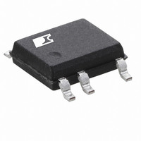
LNK306DG Power Integrations, LNK306DG Datasheet - Page 3

LNK306DG
Manufacturer Part Number
LNK306DG
Description
IC OFFLINE SWIT OCP 8SOP
Manufacturer
Power Integrations
Series
LinkSwitch®-TNr
Type
Off Line Switcherr
Datasheet
1.LNK302GN-TL.pdf
(20 pages)
Specifications of LNK306DG
Output Isolation
Non-Isolated
Frequency Range
62 ~ 70kHz
Voltage - Output
700V
Power (watts)
12mW
Operating Temperature
-40°C ~ 150°C
Package / Case
8-SOIC (0.154", 3.90mm Width) 7 leads
For Use With
596-1127 - KIT REF DESIGN LED LINKSWITCH TN
Lead Free Status / RoHS Status
Lead free / RoHS Compliant
Available stocks
Company
Part Number
Manufacturer
Quantity
Price
Part Number:
LNK306DG-TL
Manufacturer:
POWER
Quantity:
20 000
Company:
Part Number:
LNK306DG-TL
Manufacturer:
POWER
Quantity:
4 999
Company:
Part Number:
LNK306DG-TL
Manufacturer:
POWER
Quantity:
13 506
Pin Functional Description
DRAIN (D) Pin:
Power MOSFET drain connection. Provides internal operating
current for both start-up and steady-state operation.
BYPASS (BP) Pin:
Connection point for a 0.1 μF external bypass capacitor for the
internally generated 5.8 V supply.
FEEDBACK (FB) Pin:
During normal operation, switching of the power MOSFET is
controlled by this pin. MOSFET switching is terminated when
a current greater than 49 μA is delivered into this pin.
SOURCE (S) Pin:
This pin is the power MOSFET source connection. It is also the
ground reference for the BYPASS and FEEDBACK pins.
Figure 3. Pin Confi guration.
LinkSwitch-TN Functional
Description
LinkSwitch-TN combines a high voltage power MOSFET switch
with a power supply controller in one device. Unlike conventional
PWM (pulse width modulator) controllers, LinkSwitch-TN uses
a simple ON/OFF control to regulate the output voltage. The
LinkSwitch-TN controller consists of an oscillator, feedback
(sense and logic) circuit, 5.8 V regulator, BYPASS pin under-
voltage circuit, over-temperature protection, frequency jittering,
current limit circuit, leading edge blanking and a 700 V power
MOSFET. The LinkSwitch-TN incorporates additional circuitry
for auto-restart.
Oscillator
The typical oscillator frequency is internally set to an average
of 66 kHz. Two signals are generated from the oscillator: the
maximum duty cycle signal (DC
indicates the beginning of each cycle.
BP
FB
G Package (SMD-8B)
P Package (DIP-8B)
S
S
1
2
3
4
3a
8
7
5
S
S
D
MAX
D Package (SO-8C)
BP
FB
) and the clock signal that
D
1
2
4
3b
PI-3491-120706
8
7
6
5
S
S
S
S
The LinkSwitch-TN oscillator incorporates circuitry that
introduces a small amount of frequency jitter, typically 4 kHz
peak-to-peak, to minimize EMI emission. The modulation rate
of the frequency jitter is set to 1 kHz to optimize EMI reduction
for both average and quasi-peak emissions. The frequency
jitter should be measured with the oscilloscope triggered at
the falling edge of the DRAIN waveform. The waveform in
Figure 4 illustrates the frequency jitter of the LinkSwitch-TN.
Feedback Input Circuit
The feedback input circuit at the FB pin consists of a low
impedance source follower output set at 1.65 V. When the current
delivered into this pin exceeds 49 μA, a low logic level (disable)
is generated at the output of the feedback circuit. This output
is sampled at the beginning of each cycle on the rising edge of
the clock signal. If high, the power MOSFET is turned on for
that cycle (enabled), otherwise the power MOSFET remains off
(disabled). Since the sampling is done only at the beginning of
each cycle, subsequent changes in the FB pin voltage or current
during the remainder of the cycle are ignored.
5.8 V Regulator and 6.3 V Shunt Voltage Clamp
The 5.8 V regulator charges the bypass capacitor connected to
the BYPASS pin to 5.8 V by drawing a current from the voltage
on the DRAIN, whenever the MOSFET is off. The BYPASS
pin is the internal supply voltage node for the LinkSwitch-TN.
When the MOSFET is on, the LinkSwitch-TN runs off of the
energy stored in the bypass capacitor. Extremely low power
consumption of the internal circuitry allows the LinkSwitch-TN
to operate continuously from the current drawn from the DRAIN
pin. A bypass capacitor value of 0.1 μF is suffi cient for both
high frequency decoupling and energy storage.
In addition, there is a 6.3 V shunt regulator clamping the
BYPASS pin at 6.3 V when current is provided to the BYPASS
pin through an external resistor. This facilitates powering of
LinkSwitch-TN externally through a bias winding to decrease
the no-load consumption to about 50 mW.
BYPASS Pin Under-Voltage
The BYPASS pin under-voltage circuitry disables the power
MOSFET when the BYPASS pin voltage drops below 4.85 V.
Once the BYPASS pin voltage drops below 4.85 V, it must rise
back to 5.8 V to enable (turn-on) the power MOSFET.
Over-Temperature Protection
The thermal shutdown circuitry senses the die temperature.
The threshold is set at 142 °C typical with a 75 °C hysteresis.
When the die temperature rises above this threshold (142 °C) the
power MOSFET is disabled and remains disabled until the die
temperature falls by 75 °C, at which point it is re-enabled.
Current Limit
The current limit circuit senses the current in the power MOSFET.
When this current exceeds the internal threshold (I
LNK302/304-306
LIMIT
Rev. I 11/08
2-3
), the
3


