TNY268GN Power Integrations, TNY268GN Datasheet - Page 2
TNY268GN
Manufacturer Part Number
TNY268GN
Description
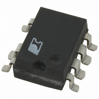
IC OFFLINE SWIT OTP OCP HV 8SMD
Manufacturer
Power Integrations
Series
TinySwitch®-IIr
Datasheet
1.TNY264GN-TL.pdf
(22 pages)
Specifications of TNY268GN
Output Isolation
Isolated
Frequency Range
124 ~ 140kHz
Voltage - Output
700V
Power (watts)
23W
Operating Temperature
-40°C ~ 150°C
Package / Case
8-SMD Gull Wing, 7 Leads
Output Voltage
5.8 V
Input / Supply Voltage (max)
265 VAC
Input / Supply Voltage (min)
85 VAC
Duty Cycle (max)
68 %
Switching Frequency
132 KHz
Supply Current
380 uA
Operating Temperature Range
- 40 C to + 150 C
Mounting Style
SMD/SMT
Lead Free Status / RoHS Status
Lead free / RoHS Compliant
Available stocks
Company
Part Number
Manufacturer
Quantity
Price
Company:

Part Number:
TNY268GN
Manufacturer:
PowerInt
Quantity:
950
Part Number:
TNY268GN
Manufacturer:
POWER
Quantity:
20 000
Company:
Part Number:
TNY268GN-TL
Manufacturer:
PowerInt
Quantity:
24 000
Company:
Part Number:
TNY268GN-TL
Manufacturer:
TI
Quantity:
1 707
Part Number:
TNY268GN-TL
Manufacturer:
POWER
Quantity:
20 000


Pin Functional Description
DRAIN (D) Pin:
Power MOSFET drain connection. Provides internal operating
current for both start-up and steady-state operation.
BYPASS (BP) Pin:
Connection point for a 0.1 μF external bypass capacitor for the
internally generated 5.8 V supply.
ENABLE/UNDERVOLTAGE (EN/UV) Pin:
This pin has dual functions: enable input and line undervoltage
sense. During normal operation, switching of the power
MOSFET is controlled by this pin. MOSFET switching is
terminated when a current greater than 240 μA is drawn from
this pin. This pin also senses line undervoltage conditions
through an external resistor connected to the DC line voltage.
If there is no external resistor connected to this pin,
TinySwitch-II detects its absence and disables the line
undervoltage function.
SOURCE (S) Pin:
Control circuit common, internally connected to output
MOSFET source.
Rev. H 02/09
Figure 2.
VOLTAGE
ENABLE/
UNDER-
(EN/UV)
240 A
2
BYPASS
(BP)
Functional Block Diagram.
TNY263-268
ENABLE
1.0 V + V T
1.0 V
50 A
6.3 V
OSCILLATOR
LINE UNDER-VOLTAGE
JITTER
COUNTER
RESTART
DC MAX
AUTO-
CLOCK
RESET
PRESENT
FAULT
Figure 3.
SOURCE (HV RTN) Pin:
Output MOSFET source connection for high voltage return.
LIMIT STATE
CURRENT
MACHINE
Pin Confi guration.
S
R
SHUTDOWN
THERMAL
5.8 V
4.8 V
Q
Q
EN/UV
BP
G Package (SMD-8B)
+
-
P Package (DIP-8B)
S
S
BYPASS PIN
UNDER-VOLTAGE
1
2
3
4
REGULATOR
5.8 V
BLANKING
CURRENT LIMIT
COMPARATOR
LEADING
EDGE
8
7
5
V I
LIMIT
S (HV RTN)
S (HV RTN)
D
www.powerint.com
+
-
PI-2643-030701
PI-2685-101600
SOURCE
DRAIN
(D)
(S)
Related parts for TNY268GN
Image
Part Number
Description
Manufacturer
Datasheet
Request
R

Part Number:
Description:
SOP-16
Manufacturer:
Power Integrations
Datasheet:
Part Number:
Description:
DIP8
Manufacturer:
Power Integrations
Datasheet:
Part Number:
Description:
TO-263
Manufacturer:
Power Integrations
Datasheet:
Part Number:
Description:
TO-263
Manufacturer:
Power Integrations
Datasheet:
Part Number:
Description:
Manufacturer:
Power Integrations
Datasheet: