TEA1752T/N1,518 NXP Semiconductors, TEA1752T/N1,518 Datasheet
TEA1752T/N1,518
Specifications of TEA1752T/N1,518
Available stocks


Related parts for TEA1752T/N1,518


TEA1752T/N1,518 Summary of contents
Page 1
... Distinctive features Integrated PFC and flyback controller Universal mains supply operation (70 V (AC) to 276 V (AC)) Dual boost PFC with accurate maximum output voltage (NXP Semiconductors patented, US patent number: US7575280) High level of integration, resulting in a very low external component count and a ...
Page 2
... Protection features Safe restart mode for system fault conditions Continuous mode protection by means of demagnetization detection for both converters (NXP Semiconductors patented, patent number: US5032967) UnderVoltage Protection (UVP) (foldback during overload) Accurate OverVoltage Protection (OVP) for PFC Accurate, adjustable OverVoltage Protection (OVP) for flyback converter ...
Page 3
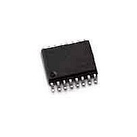
... NXP Semiconductors 4. Ordering information Table 1. Ordering information Type number Package Name Description TEA1752T SO16 plastic small outline package; 16 leads; body width 3.9 mm TEA1752LT SO16 plastic small outline package; 16 leads; body width 3.9 mm TEA1752T_LT Product data sheet TEA1752T; TEA1752LT All information provided in this document is subject to legal disclaimers. ...
Page 4
... NXP Semiconductors 5. Block diagram 1.12 V 3.5 V low Vin VINSENSE 7 boost MAXIMUM latch reset PFCCOMP 6 clamp 3.7 V VOSENSE 9 2. μA 3.5 V boost low Vin V OVP o V start flyback o V short o OCP PFC driver BLANK 500 mV PFCSENSE 11 enable PFC 60 μA SOFT START ...
Page 5
... NXP Semiconductors 6. Pinning information 6.1 Pinning Fig 2. Pin configuration: TEA1752(L)T (SOT109-1) 6.2 Pin description Table 2. Symbol V CC GND FBCTRL FBAUX LATCH PFCCOMP VINSENSE PFCAUX VOSENSE FBSENSE PFCSENSE PFCDRIVER FBDRIVER PFCTIMER HVS HV TEA1752T_LT Product data sheet TEA1752T; TEA1752LT GND FBCTRL 3 FBAUX 4 TEA1752(L)T ...
Page 6
... NXP Semiconductors 7. Functional description 7.1 General control The TEA1752(L)T contains controllers for a power factor correction circuit and for a flyback circuit. A typical configuration is shown in R AUX1 PFCDRIVER 12 PFCAUX 8 PFCCOMP 6 compensation VINSENSE 7 FBCTRL 3 R LOOP C TIMEOUT Fig 3. Typical configuration 7.1.1 Start-up and UnderVoltage LockOut (UVLO) ...
Page 7
... NXP Semiconductors converter is also activated (providing the soft start capacitor on the FBSENSE pin is charged). The flyback converter output voltage is then regulated to its nominal value. The IC supply is taken over by the auxiliary winding of the flyback converter. See If during start-up the LATCH pin does not reach the V ...
Page 8
... NXP Semiconductors VINSENSE PFCCOMP LATCH PROTECTION PFCSENSE PFCDRIVER FBSENSE FBDRIVER FBCTRL VOSENSE Fig 4. Start-up sequence, normal operation and restart sequence 7.1.2 Supply management All internal control voltages are derived from a temperature compensated and trimmed on-chip band gap circuit. Internal reference currents are derived from a temperature compensated and trimmed on-chip current reference circuit ...
Page 9
... NXP Semiconductors At initial start-up the switching is inhibited until the capacitor on the LATCH pin is charged above 1.35 V (typical). No internal filtering is carried out on this pin. An internal zener clamp of 2.9 V (typical) protects this pin from excessive voltages. 7.1.4 Fast latch reset In a typical application the mains supply can be interrupted briefly to reset the latched protection ...
Page 10
... NXP Semiconductors It is advisable to add a 5 kΩ series resistor to this pin to provide surge protection for the internal circuitry against events such as lightning surge. To prevent incorrect switching due to external disturbance, this resistor should be placed as close as possible to the IC on the printed-circuit board. 7.2.3 Frequency limitation ...
Page 11
... NXP Semiconductors Fig 5. Soft start-up of PFC 7.2.6 Low power mode When the output power of the flyback converter (see converter switches to frequency reduction mode. When the internal switching frequency limit of the flyback drops below 48 kHz (typical), the power factor correction circuit is switched off to maintain high efficiency. The switch-off can be delayed by connecting a ...
Page 12
... NXP Semiconductors Fig 6. PFC start/stop via PFCTIMER pin 7.2.8 Dual boost PFC The PFC output voltage depends on the mains input voltage. The mains input voltage is measured via the VINSENSE pin. Current is sourced from the VOSENSE pin if the voltage on the VINSENSE pin drops below 2.2 V (typical). To ensure a stable switch-over, a 200 mV transition region is inserted around the 2.2 V, see For low VINSENSE input voltages, the output current is 15 μ ...
Page 13
... NXP Semiconductors The voltage on pin VINSENSE is clamped to a minimum value, V start(VINSENSE) after a mains dropout. 7.2.11 Overvoltage protection (VOSENSE pin) An overvoltage protection circuit is incorporated to prevent output overvoltage during load steps and mains transients. When voltage on the VOSENSE pin exceeds the V power factor correction circuit is inhibited. Switching of the PFC recommences when the ...
Page 14
... NXP Semiconductors switching frequency Fig 8. Multimode operation flyback At high output power the converter switches to quasi-resonant mode. The next converter stroke is started after demagnetization of the transformer current. In quasi-resonant mode switching losses are minimized as the converter only switches on when the voltage across the external MOSFET is at its minimum (valley switching, see ...
Page 15
... NXP Semiconductors Fig 9. Frequency control of flyback part 7.3.2 Valley switching (HV pin) Figure 10 shows that a new cycle starts when the external MOSFET is activated. After the on-time (determined by the FBSENSE voltage and the FBCTRL voltage), the MOSFET is switched off and the secondary stroke starts. After the secondary stroke, the drain voltage ...
Page 16
... NXP Semiconductors (1) Start of new cycle at lowest drain voltage. (2) Start of new cycle in a classical Pulse Width Modulation (PWM) system without valley detection. Fig 10. Signals for valley switching 7.3.3 Current mode control (FBSENSE pin) Current mode control is used for the flyback converter for its good line regulation. ...
Page 17
... NXP Semiconductors Fig 11. Peak current control of flyback part 7.3.4 Demagnetization (FBAUX pin) The system is always in quasi-resonant or discontinuous conduction mode. The internal oscillator does not start a new primary stroke until the previous secondary stroke has ended. Demagnetization features a cycle-by-cycle output short circuit protection by immediately lowering the frequency (longer off-time), thus reducing the power level ...
Page 18
... NXP Semiconductors Fig 12. Time-out protection circuit Fig 13. Time-out protection (signals), safe restart in the TEA1752T Fig 14. Time-out protection (signals), latched in the TEA1752LT 7.3.6 Soft start-up (pin FBSENSE) To prevent audible transformer noise during start-up, the transformer peak current is slowly increased by the soft start function. This can be achieved by inserting a resistor ...
Page 19
... NXP Semiconductors An internal current source charges the capacitor approximately 0.63 V. The start level and the time constant of the increasing primary current level can be externally adjusted by changing the values of R τsoftstart The soft start current I voltage on pin FBSENSE has reached 0.63 V the flyback converter starts switching. ...
Page 20
... NXP Semiconductors The output voltage V demagnetization resistor OVP where N is the number of secondary turns and N s transformer. The current I The value of R accurate OVP detection possible. 7.3.9 Overcurrent protection (FBSENSE pin) The primary peak current in the transformer is accurately measured cycle-by-cycle using ...
Page 21
... NXP Semiconductors Fig 17. Overpower protection curve 7.3.11 Driver (pin FBDRIVER) The driver circuit to the gate of the external power MOSFET has a current sourcing capability of typically −500 mA and a current sink capability of typically 1.2 A. This enables fast turn-on and turn-off of the power MOSFET for efficient operation. ...
Page 22
... NXP Semiconductors Table 3. In accordance with the Absolute Maximum Rating System (IEC 60134). Symbol I PFCDRIVER I HV General P tot T stg T j ESD V ESD [1] Equivalent to discharging a 100 pF capacitor through a 1.5 kΩ series resistor. Equivalent to discharging a 200 pF capacitor through a 0.75 μH coil and a 10 Ω resistor. ...
Page 23
... NXP Semiconductors Table 5. Characteristics …continued ° all voltages are measured with respect to ground (pin 2); currents are positive when flowing into amb CC the IC; unless otherwise specified. Symbol Parameter V start-up voltage startup V undervoltage lockout threshold th(UVLO) voltage V hysteresis of start voltage start(hys) V hysteresis voltage ...
Page 24
... NXP Semiconductors Table 5. Characteristics …continued ° all voltages are measured with respect to ground (pin 2); currents are positive when flowing into amb CC the IC; unless otherwise specified. Symbol Parameter Pulse width modulator PFC t PFC on-time on(PFC) Output voltage sensing PFC (pin VOSENSE) V open-loop threshold voltage on ...
Page 25
... NXP Semiconductors Table 5. Characteristics …continued ° all voltages are measured with respect to ground (pin 2); currents are positive when flowing into amb CC the IC; unless otherwise specified. Symbol Parameter I protection current on pin prot(PFCAUX) PFCAUX PFC off delay (pin PFCTIMER) I source current on pin source(PFCTIMER) ...
Page 26
... NXP Semiconductors Table 5. Characteristics …continued ° all voltages are measured with respect to ground (pin 2); currents are positive when flowing into amb CC the IC; unless otherwise specified. Symbol Parameter Peak current control flyback (pin FBCTRL) V voltage on pin FBCTRL FBCTRL V time-out voltage on pin to(FBCTRL) ...
Page 27
... NXP Semiconductors Table 5. Characteristics …continued ° all voltages are measured with respect to ground (pin 2); currents are positive when flowing into amb CC the IC; unless otherwise specified. Symbol Parameter LATCH input (pin LATCH) V protection voltage on pin prot(LATCH) LATCH I output current on pin LATCH O(LATCH) ...
Page 28
... NXP Semiconductors 11. Application information A power supply with the TEA1752(L)T consists of a power factor correction circuit followed by a flyback converter (See Capacitor C rectified mains supply during start-up and via the auxiliary winding of the flyback converter during operation. Sense resistors R MOSFETs S1 and S2 into a voltage on pins PFCSENSE and FBSENSE. The values of ...
Page 29
... NXP Semiconductors R AUX1 PFCDRIVER 12 PFCAUX 8 PFCCOMP 6 compensation VINSENSE 7 FBCTRL 3 R LOOP C TIMEOUT Fig 18. Typical application diagram TEA1752(L)T TEA1752T_LT Product data sheet TEA1752T; TEA1752LT SS1 R SS1 R SENSE1 R S1 PFCSENSE VOSENSE HV FBTIMER TEA1752(L GND PFCTIMER All information provided in this document is subject to legal disclaimers. ...
Page 30
... NXP Semiconductors 12. Package outline SO16: plastic small outline package; 16 leads; body width 3 pin 1 index 1 e DIMENSIONS (inch dimensions are derived from the original mm dimensions) A UNIT max. 0.25 1.45 0.49 mm 1.75 0.25 0.10 1.25 0.36 0.010 0.057 0.019 inches 0.069 0.01 0.004 ...
Page 31
... NXP Semiconductors 13. Revision history Table 6. Revision history Document ID Release date TEA1752T_LT v.2 20100624 • Modifications Template upgraded to Rev 2.12.0 including revised legal information. • Text and drawings updated throughout entire data sheet. • Figure 1 • V stop(soft)PFC • Minimum junction temperature changed in ...
Page 32
... In no event shall NXP Semiconductors be liable for any indirect, incidental, punitive, special or consequential damages (including - without limitation - lost profits, lost savings, business interruption, costs related to the removal or ...
Page 33
... TEA1752T_LT Product data sheet TEA1752T; TEA1752LT own risk, and (c) customer fully indemnifies NXP Semiconductors for any liability, damages or failed product claims resulting from customer design and use of the product for automotive applications beyond NXP Semiconductors’ standard warranty and NXP Semiconductors’ product specifications. ...
Page 34
... NXP Semiconductors 16. Contents 1 General description . . . . . . . . . . . . . . . . . . . . . . 1 2 Features and benefits . . . . . . . . . . . . . . . . . . . . 1 2.1 Distinctive features . . . . . . . . . . . . . . . . . . . . . . 1 2.2 Green features . . . . . . . . . . . . . . . . . . . . . . . . . 1 2.3 PFC green features . . . . . . . . . . . . . . . . . . . . . 2 2.4 Flyback green features . . . . . . . . . . . . . . . . . . . 2 2.5 Protection features . . . . . . . . . . . . . . . . . . . . . . 2 3 Applications . . . . . . . . . . . . . . . . . . . . . . . . . . . . 2 4 Ordering information . . . . . . . . . . . . . . . . . . . . . 3 5 Block diagram . . . . . . . . . . . . . . . . . . . . . . . . . . 4 6 Pinning information . . . . . . . . . . . . . . . . . . . . . . 5 6.1 Pinning . . . . . . . . . . . . . . . . . . . . . . . . . . . . . . . 5 6.2 Pin description . . . . . . . . . . . . . . . . . . . . . . . . . 5 7 Functional description ...