TNY256PN Power Integrations, TNY256PN Datasheet
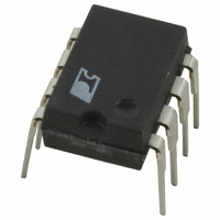
IC OFFLINE SWIT OTP UVLO HV 8DIP

TNY256PN

Manufacturer Part Number
TNY256PN
Description
IC OFFLINE SWIT OTP UVLO HV 8DIP
Manufacturer
Power Integrations
Series
TinySwitch® Plusr
Datasheet

Specifications of TNY256PN

Output Isolation
Isolated
Frequency Range
115 ~ 140kHz
Voltage - Output
700V
Power (watts)
10W
Operating Temperature
-40°C ~ 150°C
Package / Case
8-DIP (0.300", 7.62mm)
Output Voltage
5.8 V
Input / Supply Voltage (max)
265 VAC
Input / Supply Voltage (min)
85 VAC
Duty Cycle (max)
69 %
Switching Frequency
130 KHz
Supply Current
255 uA
Operating Temperature Range
- 40 C to + 150 C
Mounting Style
Through Hole
Lead Free Status / RoHS Status
Lead free / RoHS Compliant
Other names
596-1171-5
TNY256PN

Available stocks

Company
Part Number
Manufacturer
Quantity
Price
Part Number:
TNY256PN
Manufacturer:
POWER
Quantity:
3 000
Part Number:
TNY256PN
Manufacturer:
POWER
Quantity:
15 000
Part Number:
TNY256PN
Manufacturer:
POWER
Quantity:
20 000
Company:
Part Number:
TNY256PN
Quantity:
21 000
TNY256
TinySwitch
Energy Efficient, Low Power Off-line Switcher
TinySwitch Plus Features
• Extended power range
• Fully integrated auto-restart reduces short circuit current
• Line under-voltage sense eliminates turn-off glitches
• Frequency jittering dramatically reduces EMI (5 to 10 dB)
• TO-220 package option
Lowest Cost, Low Power Switcher Solution
• Lower cost than RCC, discrete PWM and other
• Cost effective replacement for bulky linear adapters
• Lowest component count
• Simple ON/OFF control – no loop compensation components
• No bias winding – simpler, lower cost transformer
• Designed to work with low cost external components
Extremely Energy Efficient
• Consumes only 30/60 mW at 115/230 VAC with no load
• Meets Blue Angel, Energy Star, Energy 2000 and
• Saves $1 to $4 per year in energy costs (at $0.12/kWHr)
• Ideal for cellular phone chargers and adapters
High Performance at Low Cost
• High voltage powered – ideal for charger applications
• High bandwidth provides fast turn on with no overshoot
• Current limit operation rejects line frequency ripple
• Built-in current limit and thermal protection
Description
The TNY256 extends the power range of the TinySwitch family
of energy efficient, low power off-line switchers. TinySwitch
devices use a breakthrough design to provide the lowest cost,
high efficiency, off-line switching solution for low power
applications. They integrate a 700 V power MOSFET, oscillator,
high voltage switched current source, current limit and thermal
shutdown circuitry into a single, monolithic device. The
devices start-up and operate on power derived from the DRAIN
voltage, eliminating the need for a transformer bias winding and
associated circuitry. TinySwitch's low operating current allows
power supply no-load consumption to be kept under 100 mW,
even at 265 VAC input.
integrated/hybrid solutions
200mW European cell phone requirements for standby
compared to bulky linear adapters
Product Highlights
®
Plus
Figure 1. Typical Standby Application.
The TinySwitch Plus incorporates auto-restart, line under-voltage
sense, and frequency jittering features. The auto-restart circuit
safely limits output power during fault conditions such as output
short or open loop. The auto-restart circuit is fully integrated and
does not require external timing components. The line under-
voltage sense threshold can be externally programmed using a line
sense resistor. During start-up, this feature keeps the TNY256 off
until the input line voltage reaches the under-voltage threshold.
When the input line voltage is removed, the line under-voltage
circuit prevents auto-restart attempts after the output goes out of
regulation. This eliminates power down glitches caused by the
slow discharge of input storage capacitors present in applications
such as standby supplies. A single resistor is used to implement
this feature, eliminating what normally takes five to six components.
The line sense resistor is optional. The TNY256 operating frequency
of 130 kHz is jittered (frequency modulated) to reduce both quasi-
peak and average EMI, minimizing filtering costs.
Table 1. * The low end of the power ranges shown represent enclosed
adapters with minimal heat sinking whereas, the high end of the power
ranges represent open frame power supplies with adequate heat
sinking, both measured at an ambient of 50
Application Considerations section for more details.
TinySwitch Plus
TNY256G
TNY256Y
Wide-Range
HV DC Input
TNY256P
NUMBER
ORDER
+
PART
OUTPUT POWER CAPABILITY*
TO-220-7B
PACKAGE
SMD-8
DIP-8
UV Resistor
Optional
D
S
EN/UV
BP
230 VAC or
w/Doubler
115 VAC
8-19 W
8-15 W
o
C. Please refer to the Key
85-265
DC Output
5-11 W
PI-2363-022699
5-10 W
VAC
July 2001
+
®

Related parts for TNY256PN

TNY256PN Summary of contents

Page 1

TNY256 TinySwitch Energy Efficient, Low Power Off-line Switcher Product Highlights TinySwitch Plus Features • Extended power range • Fully integrated auto-restart reduces short circuit current • Line under-voltage sense eliminates turn-off glitches • Frequency jittering dramatically reduces EMI (5 to ...

Page 2

TNY256 BYPASS (BP) LINE UNDER-VOLTAGE OSCILLATOR ENABLE/ UNDER-VOLTAGE 1.5 V (EN/UV) Figure 2. Functional Block Diagram. Pin Functional Description DRAIN (D) Pin: Power MOSFET drain connection. Provides internal operating current for both start-up ...

Page 3

TinySwitch Functional Description TinySwitch combines a high voltage power MOSFET switch with a power supply controller in one device. Unlike conventional PWM (Pulse Width Modulator) controllers, TinySwitch uses a simple ON/OFF control to regulate the output voltage. The TNY256 controller ...

Page 4

TNY256 short open loop condition, TNY256 enters into auto- restart operation. An internal counter clocked by the oscillator gets reset every time the EN/UV pin is pulled low. If the EN/ UV pin is not pulled low for ...

Page 5

V 100 DC-BUS BYPASS 0 400 200 V DRAIN Time (ms) Figure 8. TNY256 Power-up With External Resistor ( Connected to EN/UV Pin. power level at the lowest input voltage, ...

Page 6

TNY256 200 V 100 0 400 300 V 200 100 Time (s) Figure 10. Normal Power-down Timing. During power-down, when an external resistor is used, the power MOSFET will switch for 32 ms after the output loses ...

Page 7

L1 470 1N4005 1N4005 4.7 k 85-265 RF1 C1 C2 VAC 400 V 400 V Fusible D3 D4 1N4005 1N4005 Figure 12. 5 Adapter with Universal Input (85-265 VAC). ...

Page 8

TNY256 Layout Single Point Grounding Use a single point ground connection at the SOURCE pin for the BYPASS pin capacitor and the Input Filter Capacitor (see Figure 13). Primary Loop Area The area of the primary loop that connects the ...

Page 9

DRAIN Voltage ....................................... - 0 700 V Peak DRAIN Current ............................................. 800 mA EN/UV Voltage ............................................ - 0 EN/UV Current ...................................................... 100 mA 1. All voltages referenced to SOURCE Normally limited by ...

Page 10

TNY256 Parameter Symbol CONTROL FUNCTIONS (cont.) BYPASS Pin V Voltage BP BYPASS V Hysteresis BPH EN/UV Pin Line I Under-voltage LUV Threshold CIRCUIT PROTECTION I Current Limit LIMIT Initial Current I Limit INIT Leading Edge t LEB Blanking Time Current ...

Page 11

Parameter Symbol OUTPUT (cont.) DRAIN Supply Voltage Output EN/UV t Delay EN/UV Output Disable t Setup Time DST Auto-Restart t AR ON-Time Auto-Restart DC Duty Cycle AR NOTES: A. For a threshold with a negative value, negative hysteresis is a ...

Page 12

TNY256 D EN/ NOTE: This test circuit is not applicable for current limit or output characteristic measurements. Figure 14. TinySwitch General Test Circuit 90% DRAIN VOLTAGE 10 ...

Page 13

Typical Performance Characteristics BREAKDOWN vs. TEMPERATURE 1.1 1.0 0.9 -50 - 100 125 150 Junction Temperature ( C) CURRENT LIMIT vs. TEMPERATURE 1.4 1.2 1.0 0.8 0.6 0.4 0.2 0.0 -50 - Temperature ...

Page 14

TNY256 Typical Performance Characteristics (cont.) C OSS vs. DRAIN VOLTAGE 100 200 400 DRAIN Voltage ( 7/01 DRAIN CAPACITANCE POWER 100 600 0 UNDERVOLTAGE THRESHOLD 80 Power-up* 40 Power-down at ...

Page 15

DIM inches mm A 0.370-0.385 9.40-9.78 B 0.245-0.255 6.22-6.48 C 0.125-0.135 3.18-3.43 G 0.015-0.040 0.38-1.02 H 0.120-0.135 3.05-3.43 J1 0.060 (NOM) 1.52 (NOM) J2 0.014-0.022 0.36-0.56 K 0.010-0.012 0.25-0.30 L 0.090-0.110 2.29-2.79 M 0.030 (MIN) 0.76 (MIN) N 0.300-0.320 7.62-8.13 ...

Page 16

TNY256 .400 (10.16) .146 (3.71) .415 (10.54) .156 (3.96) + .860 (21.84) .880 (22.35) PIN 1 .050 (1.27) BSC .150 (3.81) BSC .050 (1.27) .050 (1.27) .050 (1.27) .200 (5.08) PIN 1 .150 (3.81) Y07B MOUNTING HOLE PATTERN C 16 ...

Page 17

Notes TNY256 C 17 7/01 ...

Page 18

TNY256 C 18 7/01 Notes ...

Page 19

Notes TNY256 C 19 7/01 ...

Page 20

... Power Integrations reserves the right to make changes to its products at any time to improve reliability or manufacturability. Power Integrations does not assume any liability arising from the use of any device or circuit described herein, nor does it convey any license under its patent rights or the rights of others. ...

Related keywords