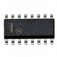
MC33363ADWR2G ON Semiconductor, MC33363ADWR2G Datasheet

MC33363ADWR2G
Specifications of MC33363ADWR2G
Available stocks
Related parts for MC33363ADWR2G
MC33363ADWR2G Summary of contents
Page 1
... ORDERING INFORMATION See detailed ordering and shipping information in the package dimensions section on page 7 of this data sheet. *For additional information on our Pb--Free strategy and soldering details, please download the ON Semiconductor Soldering and Mounting Techniques Reference Manual, SOLDERRM/D. Publication Order Number: MC33363A/D ...
Page 2
MAXIMUM RATINGS (Note 1) Power Switch (Pin 16) Drain Voltage Drain Current Startup Input Voltage (Pin 1) Power Supply Voltage (Pin 3) Input Voltage Range Voltage Feedback Input (Pin 10) Compensation (Pin 9) Overvoltage Protection Input (Pin 11) R (Pin ...
Page 3
ELECTRICAL CHARACTERISTICS values T is the operating junction temperature range that applies (Note 2), unless otherwise noted) J Characteristic ERROR AMPLIFIER (Pins 9, 10) Gain Bandwidth Product (f = 100 kHz 25C) J Output Voltage Swing High State ...
Page 4
100 pF T 500 200 pF T 200 500 1.0 nF 100 2 5 ...
Page 5
V 1.75 V 1.70 V 1.0 ms/DIV Figure 8. Error Amplifier Small Signal Transient Response 0 --20 --40 --60 --80 0 4.0 8 REGULATOR SOURCE CURRENT (mA) reg Figure 10. Regulator Output Voltage Change versus Source ...
Page 6
I = 200 8.0 4.0 Pulse tested at 5.0 ms with < 1.0% duty cycle so that close --50 -- AMBIENT TEMPERATURE (C) ...
Page 7
... This pin is designed to directly drive the converter transformer and is capable of switching a Drain maximum of 700 V and 1.0 A. ORDERING INFORMATION Device MC33363ADWG MC33363ADWR2G †For information on tape and reel specifications, including part orientation and tape sizes, please refer to our Tape and Reel Packaging Specifications Brochure, BRD8011/D. Description potential on Pin 3. CC ...
Page 8
AC Input Current Mirror Regulator Output Band Gap 6.5 V Regulator Oscillator PWM Comparator Thermal Current Limit Shutdown Comparator Gnd 4, 5, 12, 13 Capacitor C T Compensation ...
Page 9
Introduction The MC33363A represents a new higher level of integration by providing all the active high voltage power, control, and protection circuitry implementation of a flyback or forward converter on a single monolithic chip. This device is designed for direct ...
Page 10
V and 1.0 A. Proper device voltage snubbing and heatsinking are required for reliable operation. A Leading Edge Blanking circuit was placed in the current sensing signal path. This circuit prevents a premature reset of the PWM ...
Page 11
1.0 A 1N4006 92 to 276 D2 D1 Vac Input Mirror Reg PWM Latch Osc C3 7 1200 pF PWM Thermal 4, 5, 12, 13 Table 1. CONVERTER TEST DATA ...
Page 12
Caution! High C4 Voltages IC1 F1 AC Line C2 R5 Input MC33363A Figure 23. Printed Circuit Board and Component Layout (Circuit of Figure 22) http://onsemi.com IC3 ...
Page 13
... Equal Opportunity/Affirmative Action Employer. This literature is subject to all applicable copyright laws and is not for resale in any manner. PUBLICATION ORDERING INFORMATION LITERATURE FULFILLMENT: Literature Distribution Center for ON Semiconductor P.O. Box 5163, Denver, Colorado 80217 USA Phone: 303--675--2175 or 800--344--3860 Toll Free USA/Canada Fax: 303--675--2176 or 800--344--3867 Toll Free USA/Canada Email: orderlit@onsemi ...


