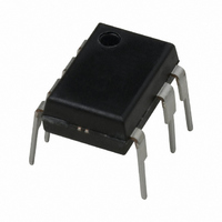
FSD210 Fairchild Semiconductor, FSD210 Datasheet

FSD210
Specifications of FSD210
FSD210_NL
Available stocks
Related parts for FSD210
FSD210 Summary of contents
Page 1
... Charger & Adaptor for Mobile Phone, PDA & MP3 • Auxiliary Power for White Goods, PC, C-TV & Monitor Description The FSD200 and FSD210 are integrated Pulse Width Modu- lators (PWM) and Sense FETs specially designed for high performance off-line Switch Mode Power Supplies (SMPS) with minimal external components ...
Page 2
... Reset Figure 4. Functional Block Diagram of FSD200 showing internal high voltage regulator 2 Internal Voltage Bias Ref 8.7/6.7V Vck OSC BURST V BURST OLP TSD A/R Figure 3. Functional Block Diagram of FSD210 Voltage UVLO Ref. Vck OSC BURST V BURST OLP TSD A/R Vstr DRIVER SFET ...
Page 3
... The startup pin connects directly to the rectified AC line voltage source for both the FSD200 and FSD210. For the FSD210, at start up the internal switch supplies internal bias and charges an external storage capacitor placed between the Vcc pin and ground. Once this reaches 8.7V, the internal current source is disabled ...
Page 4
... FSD210, FSD200 Absolute Maximum Ratings (Ta=25 C unless otherwise specified) Parameter Maximum Supply Voltage (FSD200) Maximum Supply Voltage (FSD210) Input Voltage Range Operating Junction Temperature. Operating Ambient Temperature Storage Temperature Range Thermal Impedance Parameter 7DIP Junction-to-Ambient Thermal Junction-to-Case Thermal 7LSOP Junction-to-Ambient Thermal ...
Page 5
... Leading Edge Blanking Time TOTAL DEVICE SECTION Operating Supply Current (FSD200) Operating Supply Current (FSD210) Start Up Current (FSD200) Start Up Current (FSD210) Vstr Supply Voltage Note: 1. These parameters, although guaranteed, are not 100% tested in production 2. This parameter is derived from characterization Symbol Condition ...
Page 6
... FSD210, FSD200 Comparison Between FSDH565 and FSD210 Function Soft-Start not applicable Switching Frequency 100kHz Frequency Modulation not applicable Burst Mode Operation not applicable Drain Creepage at 1.02mm Package 6 FSDH0565 FSD210 3mS 134kHz ±4kHz Yes-built into controller 3.56mm DIP 3.56mm LSOP FSD210 Advantages • ...
Page 7
... FSD210, FSD200 - 100 Junction Temperature (℃) Operating Current vs. Temp - 100 Junction Temperature (℃) Feedback Source Current vs. Temp - 100 Junction Temperature (℃) Vstop Voltage vs ...
Page 8
... Junction Temperature (℃) Vcc Regulation Voltage vs. Temp (for FSD200) 1.4 1.2 1.0 0.8 0.6 0.4 0.2 0.0 - Junction Temperature (℃) Start Up Current vs. Temp (for FSD210) 8 (Continued) 1.2 1.0 0.8 0.6 0.4 0.2 0.0 75 100 125 1.2 1.0 0.8 0.6 0.4 ...
Page 9
... The device continues to switch provided that Vcc does not drop below 6.7V. For FSD210, after startup, the bias is supplied from the auxiliary transformer winding. In the case of FSD200, Vcc is continuously supplied from the ...
Page 10
... Sense FET remains off. This causes Vcc to fall. When Vcc reaches the UVLO stop voltage (6.7V:FSD210, 6V:FSD200), the protection is reset and the internal high voltage current source charges the Vcc capaci- tor. When Vcc reaches the UVLO start voltage (8 ...
Page 11
... FSD2xx Burst Operation Block Figure 14. Frequency Modulation Waveforms time Figure 15. FSDH0165 Full Range EMI scan(100kHz, no Frequency Modulation) with charger set Figure 16. FSD210 Full Range EMI scan(134kHz, with Fre- FSD210, FSD200 Internal Oscillator 138kHz Drain to Source voltage Drain to Vds ...
Page 12
... Output power Cellular Phone Charger Features • High efficiency (>67% at Universal Input) • Low zero load power consumption (<100mW at 240Vac) with FSD210 • Low component count • Enhanced system reliability through various protection functions • Internal soft-start (3ms) • Frequency Modulation for low EMI Key Design Notes • ...
Page 13
... FSD210, FSD200 Requirement/Comment Requirement/Comment DO41 Type DO41 Type DO41 Type DO41 Type D0-213 Type D0-213 Type D0-41 Type D0-41 Type TO-92 Type TO-92 Type Iover=0.3A, Fairchildsemi Iover=0.3A, Fairchildsemi ...
Page 14
... The output voltage(12V) is regulated with resistors, R1, R2 and R3, zener diode, D3, the transistor, Q1 and the capacitor, C2. While the FSD210 is off diodes, D1 and D2, are on. At this time the output voltage, 12V, can be sensed by the feedback components above. This output is also used with bias voltage for the FSD210. ...
Page 15
... Layout Considerations (for Flyback Convertor GND #2 : GND #3 : GND #4 : Vfb #5 : Vcc # Drain #8 : Vstr Figure 17. Layout Considerations for FSD2x0 using 7DIP FSD210, FSD200 Copper area for heatsink 15 ...
Page 16
... FSD210, FSD200 Package Dimensions 16 7-DIP ...
Page 17
... Package Dimensions (Continued) 7-LSOP FSD210, FSD200 17 ...
Page 18
... FSD210, FSD200 Ordering Information Product Number FSD210 FSD200 FSD210M FSD200M DISCLAIMER FAIRCHILD SEMICONDUCTOR RESERVES THE RIGHT TO MAKE CHANGES WITHOUT FURTHER NOTICE TO ANY PRODUCTS HEREIN TO IMPROVE RELIABILITY, FUNCTION OR DESIGN. FAIRCHILD DOES NOT ASSUME ANY LIABILITY ARISING OUT OF THE APPLICATION OR USE OF ANY PRODUCT OR CIRCUIT DESCRIBED HEREIN; NEITHER DOES IT CONVEY ANY LICENSE UNDER ITS PATENT RIGHTS, NOR THE RIGHTS OF OTHERS ...


