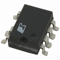
LNK306G Power Integrations, LNK306G Datasheet - Page 12

LNK306G
Manufacturer Part Number
LNK306G
Description
IC OFFLINE SWIT OCP 8SMD
Manufacturer
Power Integrations
Series
LinkSwitch®-TNr
Datasheet
1.LNK302GN-TL.pdf
(20 pages)
Specifications of LNK306G
Output Isolation
Non-Isolated
Frequency Range
62 ~ 70kHz
Voltage - Output
700V
Power (watts)
12mW
Operating Temperature
-40°C ~ 150°C
Package / Case
8-SMD Gull Wing, 7 Leads
Lead Free Status / RoHS Status
Contains lead / RoHS non-compliant
Available stocks
Company
Part Number
Manufacturer
Quantity
Price
Company:
Part Number:
LNK306GN
Manufacturer:
PowerInt
Quantity:
950
Company:
Part Number:
LNK306GN-TL
Manufacturer:
ISSI
Quantity:
760
Company:
Part Number:
LNK306GN-TL
Manufacturer:
PowerInt
Quantity:
10 494
Part Number:
LNK306GN-TL
Manufacturer:
POWER
Quantity:
20 000
Company:
Part Number:
LNK306GN-TL
Manufacturer:
POWER
Quantity:
10 616
Rev. I 11/08
NOTES:
A. Total current consumption is the sum of I
B Since the output MOSFET is switching, it is diffi cult to isolate the switching current from the supply current at the
C. See Typical Performance Characteristics section Figure 14 for BYPASS pin start-up charging waveform.
D. This current is only intended to supply an optional optocoupler connected between the BYPASS and FEEDBACK
E. For current limit at other di/dt values, refer to Figure 13.
F. This parameter is guaranteed by design.
G. This parameter is derived from characterization.
H. Auto-restart on time has the same temperature characteristics as the oscillator (inversely proportional to
Figure 7. LinkSwitch-TN General Test Circuit.
Figure 8. LinkSwitch-TN Duty Cycle Measurement.
2-12
12
switching) and the sum of I
DRAIN. An alternative is to measure the BYPASS pin current at 6 V.
frequency).
pins and not any other external circuitry.
LNK302/304-306
50 V
S2
S1
and I
DSS
when FEEDBACK pin is shorted to SOURCE (MOSFET switching).
470 Ω
5 W
S1
and I
DSS
when FEEDBACK pin voltage is ≥2 V (MOSFET not
S
S
D
FB
BP
S
S
Figure 9. LinkSwitch-TN Output Enable Timing.
(internal signal)
DC
V
DRAIN
t
P
MAX
=
FB
f
OSC
1
470 kΩ
0.1 μF
t P
t EN
S2
50 V
PI-3707-112503
PI-3490-060204


