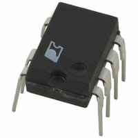
LNK306P Power Integrations, LNK306P Datasheet - Page 8

LNK306P
Manufacturer Part Number
LNK306P
Description
IC OFFLINE SWIT OCP 8DIP
Manufacturer
Power Integrations
Series
LinkSwitch®-TNr
Datasheet
1.LNK302GN-TL.pdf
(20 pages)
Specifications of LNK306P
Output Isolation
Non-Isolated
Frequency Range
62 ~ 70kHz
Voltage - Output
700V
Power (watts)
12mW
Operating Temperature
-40°C ~ 150°C
Package / Case
8-DIP (0.300", 7.62mm), 7 Leads
Lead Free Status / RoHS Status
Contains lead / RoHS non-compliant
Available stocks
Company
Part Number
Manufacturer
Quantity
Price
Company:
Part Number:
LNK306P
Manufacturer:
Chemi-con
Quantity:
30 000
Company:
Part Number:
LNK306PN
Manufacturer:
POWER
Quantity:
3 000
Company:
Part Number:
LNK306PN
Manufacturer:
PowerInt
Quantity:
9 750
Part Number:
LNK306PN
Manufacturer:
POWER
Quantity:
20 000
Pre-load Resistor R4
In high-side, direct feedback designs where the minimum load
is <3 mA, a pre-load resistor is required to maintain output
regulation. This ensures suffi cient inductor energy to pull the
inductor side of the feedback capacitor C3 to input return via
D2. The value of R4 should be selected to give a minimum
output load of 3 mA.
In designs with an optocoupler the Zener or reference bias
current provides a 1 mA to 2 mA minimum load, preventing
“pulse bunching” and increased output ripple at zero load.
LinkSwitch-TN Layout Considerations
In the buck or buck-boost converter confi guration, since the
SOURCE pins in LinkSwitch-TN are switching nodes, the copper
area connected to SOURCE should be minimized to minimize
EMI within the thermal constraints of the design.
In the boost confi guration, since the SOURCE pins are tied
to DC return, the copper area connected to SOURCE can be
maximized to improve heatsinking.
The loop formed between the LinkSwitch-TN, inductor (L1),
freewheeling diode (D1), and output capacitor (C2) should
be kept as small as possible. The BYPASS pin capacitor
C1 (Figure 6) should be located physically close to the
SOURCE (S) and BYPASS (BP) pins. To minimize direct
coupling from switching nodes, the LinkSwitch-TN should be
placed away from AC input lines. It may be advantageous to
place capacitors C4 and C5 in-between LinkSwitch-TN and the
AC input. The second rectifi er diode D4 is optional, but may
be included for better EMI performance and higher line surge
withstand capability.
Rev. I 11/08
2-8
8
LNK302/304-306
Quick Design Checklist
As with any power supply design, all LinkSwitch-TN designs
should be verifi ed for proper functionality on the bench. The
following minimum tests are recommended:
1) Adequate DC rail voltage – check that the minimum DC
2) Correct Diode Selection – UF400x series diodes are
3) Maximum drain current – verify that the peak drain current
4) Thermal check – at maximum output power, minimum
In a LinkSwitch-TN design using a buck or buck boost converter
topology, the SOURCE pin is a switching node. Oscilloscope
measurements should therefore be made with probe grounded
to a DC voltage, such as primary return or DC input rail, and
not to the SOURCE pins. The power supply input must always
be supplied from an isolated source (e.g. via an isolation
transformer).
input voltage does not fall below 70 VDC at maximum load,
minimum input voltage.
recommended only for designs that operate in MDCM at
an ambient of 70 °C or below. For designs operating in
continuous conduction mode (CCM) and/or higher ambients,
then a diode with a reverse recovery time of 35 ns or better,
such as the BYV26C, is recommended.
is below the data sheet peak drain specifi cation under
worst-case conditions of highest line voltage, maximum
overload (just prior to auto-restart) and highest ambient
temperature.
input voltage and maximum ambient temperature, verify
that the LinkSwitch-TN SOURCE pin temperature is
100 °C or below. This fi gure ensures adequate margin due
to variations in R
thermocouple meter is recommended to make measurements
when the SOURCE pins are a switching node. Alternatively,
the ambient temperature may be raised to indicate margin
to thermal shutdown.
DS(ON)
from part to part. A battery powered


