TOP242G Power Integrations, TOP242G Datasheet - Page 4
TOP242G
Manufacturer Part Number
TOP242G
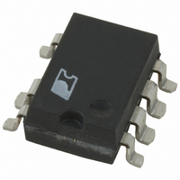
Description
IC OFFLINE SWIT OVP UVLO HV 8SMD
Manufacturer
Power Integrations
Series
TOPSwitch®-GXr
Datasheet
1.TOP242GN-TL.pdf
(52 pages)
Specifications of TOP242G
Output Isolation
Isolated
Frequency Range
66 ~ 132kHz
Voltage - Output
700V
Power (watts)
15W
Operating Temperature
-40°C ~ 150°C
Package / Case
8-SMD Gull Wing, 7 Leads
Lead Free Status / RoHS Status
Contains lead / RoHS non-compliant
Available stocks
Company
Part Number
Manufacturer
Quantity
Price
Company:

Part Number:
TOP242GN
Manufacturer:
Power Integrations
Quantity:
135
Company:
Part Number:
TOP242GN
Manufacturer:
ANV
Quantity:
5 510
Part Number:
TOP242GN
Manufacturer:
POWER
Quantity:
20 000
Company:
Part Number:
TOP242GN-TL
Manufacturer:
Power Integrations
Quantity:
66 319
Part Number:
TOP242GN-TL
Manufacturer:
POWER
Quantity:
20 000


Figure 3. Pin Configuration (top view).
Pin Functional Description
DRAIN (D) Pin:
High voltage power MOSFET drain output. The internal
start-up bias current is drawn from this pin through a switched
high-voltage current source. Internal current limit sense point
for drain current.
CONTROL (C) Pin:
Error amplifier and feedback current input pin for duty cycle
control. Internal shunt regulator connection to provide internal
bias current during normal operation. It is also used as the
connection point for the supply bypass and auto-restart/
compensation capacitor.
LINE-SENSE (L) Pin: (Y, R or F package only)
Input pin for OV, UV, line feed forward with DC
remote ON/OFF and synchronization. A connection to SOURCE
pin disables all functions on this pin.
EXTERNAL CURRENT LIMIT (X) Pin: (Y, R or F package
only)
Input pin for external current limit adjustment, remote
ON/OFF, and synchronization. A connection to SOURCE pin
disables all functions on this pin.
MULTI-FUNCTION (M) Pin: (P or G package only)
This pin combines the functions of the LINE-SENSE (L) and
EXTERNAL CURRENT LIMIT (X) pins of the Y package
into one pin. Input pin for OV, UV, line feed forward with
DC
ON/OFF and synchronization. A connection to SOURCE pin
disables all functions on this pin and makes TOPSwitch-GX
operate in simple three terminal mode (like TOPSwitch-II).
4
M
C
S
S
TOP242-250
MAX
G Package (SMD-8B)
P Package (DIP-8B)
Connected to
Tab Internally
SOURCE Pin
O
11/05
reduction, external current limit adjustment, remote
3
4
2
1
Y Package (TO-220-7C)
8
7
5
S
D
S
R Package (TO-263-7C)
F Package (TO-262-7C)
C L X S F
1 2 3 4 5
MAX
D
7
PI-2724-010802
reduction,
7 D
5 F
4 S
3 X
2 L
1 C
FREQUENCY (F) Pin: (Y, R or F package only)
Input pin for selecting switching frequency: 132 kHz if
connected to SOURCE pin and 66 kHz if connected to
CONTROL pin. The switching frequency is internally set for
fixed 132 kHz operation in P and G packages.
SOURCE (S) Pin:
Output MOSFET source connection for high voltage power
return. Primary side control circuit common and reference point.
Figure 4. Y/R/F Pkg Line Sense and Externally Set Current Limit.
Figure 5. P/G Package Line Sense.
Figure 6. P/G Package Externally Set Current Limit.
Voltage
Voltage
Voltage
Input
Input
Input
DC
DC
DC
+
+
+
-
-
-
R
IL
D
S
D
S
D
S
R
R
CONTROL
CONTROL
CONTROL
LS
LS
X
12 kΩ
M
R
M
L
2 MΩ
IL
2 MΩ
C
C
C
For R
DC
DC
For R
For R
See Figures 54b, 55b
and 56b for other resistor
values (R
different I
For R
DC
DC
V
V
V
V
For R
I
See Figure 54b for
other resistor values
(R
I
V
V
V
V
LIMIT
LIMIT
MAX
MAX
MAX
MAX
UV
OV
UV
OV
UV
OV
I
I
UV
OV
IL
LIMIT
LIMIT
LS
IL
IL
LS
) to select different
= I
= I
= 100 VDC
= 450 VDC
@100 VDC = 78%
@375 VDC = 38%
@100 VDC = 78%
@375 VDC = 38%
= I
= I
= 100 VDC
= 450 VDC
= 12 kΩ
= 25 kΩ
= 69%
values
IL
= 2 MΩ
= 2 MΩ
OV
UV
LIMIT
IL
OV
UV
= 12 kΩ
= 69%
= 43%
) to select
x R
x R
PI-2517-022604
x R
x R
PI-2509-040501
values.
LS
LS
LS
LS
Related parts for TOP242G
Image
Part Number
Description
Manufacturer
Datasheet
Request
R

Part Number:
Description:
IC OFFLINE CTRLR SMPS CM TO220
Manufacturer:
Infineon Technologies
Datasheet:

Part Number:
Description:
IC OFFLINE CTRLR SMPS CM TO220
Manufacturer:
Infineon Technologies
Datasheet:

Part Number:
Description:
SOP-16
Manufacturer:
Power Integrations
Datasheet:
Part Number:
Description:
DIP8
Manufacturer:
Power Integrations
Datasheet:
Part Number:
Description:
TO-263
Manufacturer:
Power Integrations
Datasheet: