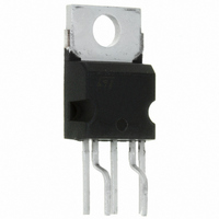
VIPER100A STMicroelectronics, VIPER100A Datasheet - Page 16

VIPER100A
Manufacturer Part Number
VIPER100A
Description
IC SWIT PWM SMPS CM PENTAWATT5
Manufacturer
STMicroelectronics
Series
VIPER™r
Specifications of VIPER100A
Output Isolation
Isolated
Frequency Range
90 ~ 200kHz
Voltage - Input
8 ~ 15 V
Voltage - Output
700V
Power (watts)
82W
Operating Temperature
25°C ~ 125°C
Package / Case
Pentawatt-5 HV (Bent and Staggered Leads)
Number Of Outputs
1
Output Voltage
700 V
Output Current
3000 mA
Mounting Style
Through Hole
Switching Frequency
90 KHz to 110 KHz
Operating Supply Voltage
0 V to 15 V
Fall Time
100 ns
Rise Time
50 ns
Synchronous Pin
No
Lead Free Status / RoHS Status
Contains lead / RoHS non-compliant
Other names
497-2712-5
Available stocks
Company
Part Number
Manufacturer
Quantity
Price
Company:
Part Number:
VIPER100A
Manufacturer:
ST
Quantity:
4 000
Part Number:
VIPER100A
Manufacturer:
ST
Quantity:
20 000
Company:
Part Number:
VIPER100A-E
Manufacturer:
ST
Quantity:
101
Company:
Part Number:
VIPER100ASP
Manufacturer:
ST
Quantity:
1 450
Part Number:
VIPER100ASP
Manufacturer:
ST
Quantity:
20 000
Company:
Part Number:
VIPER100ASPTR-E
Manufacturer:
STMicroelectronics
Quantity:
1 785
Company:
Part Number:
VIPER100ASPTRE
Manufacturer:
INF
Quantity:
4 037
Transconductance Error Amplifier
The VIPer100/100A includes a transconductance error amplifier. Transconductance Gm is the change in
output current (I
The output impedance Z
This last equation shows that the open loop gain A
A
where G
G
impedance Z can be connected between the COMP pin and ground in order to define the transfer
function F of the error amplifier more accurately, according to the following equation (very similar to the
one above):
F
The error amplifier frequency response is reported in figure 10 page 8 for different values of a simple
resistance connected on the COMP pin. The unloaded transconductance error amplifier shows an
internal Z
different compensation level. A capacitor will provide an integrator function, thus eliminating the DC static
error, and a resistance in series leads to a flat gain at higher frequency, insuring a correct phase margin.
This configuration is illustrated in (see Figure 21) page 17.
As shown in (see Figure 21) an additional noise filtering capacitor of 2.2nF is generally needed to avoid
any high frequency interference.
Is also possible to implement a slope compensation when working in continuous mode with duty cycle
higher than 50%. (see Figure 22) shows such a configuration. Note: R1 and C2 build the classical
compensation network, and Q1 is injecting the slope compensation with the correct polarity from the
oscillator sawtooth.
External Clock Synchronization:
The OSC pin provides a synchronisation capability when connected to an external frequency source.
(see Figure 23) page17 shows one possible schematic to be adapted, depending the specific needs. If
the proposed schematic is used, the pulse duration must be kept at a low value (500ns is sufficient) for
minimizing consumption. The optocoupler must be able to provide 20mA through the optotransistor.
Primary Peak Current Limitation
The primary I
shown in (see Figure 24) page 18. The circuit based on Q1, R
pin in order to limit the primary peak current of the device to a value:
where:
The suggested value for R
16/24
VOL
(S)
m
V COM P
is defined by specification, but Z
= Gm x Z(S)
= G
m
m
COMP
value for VIPer100/100A is 1.5 mA/V typically.
x Z
=
0.6
DPEAK
COMP
of about 330KΩ. More complex impedance can be connected on the COMP pin to achieve
COMP
×
R 1
- --- -- - --- -- - -- - -- - -
R
+
current and, consequently, the output power can be limited using the simple circuit
2
) versus change in input voltage (V
R 2
COMP
1
+R
2
at the output of this amplifier (COMP pin) can be defined as:
is in the range of 220KΩ.
Z
CO MP
COMP
=
∂ V COMP
-- - -- --- - -- - -- --- - -- - --- - -
∂ I CO MP
G
m
and therefore A
=
∂ I C OM P
-- - -- - -- - --- -- - -- - -- - -- -
∂ V DD
VOL
=
-- - --- -- -
G
1
m
can be related to G
DD
×
∂ V COMP
- -- --- - -- - -- --- - -- - --- -- - -
). Thus:
∂ V DD
1
VOL
and R
are subject to large tolerances. An
VIPer100/SP - VIPer100A/ASP
2
clamps the voltage on the COMP
I
D PEAK
m
and Z
=
COMP
V C OM P
- -- - -- - -- - --- -- --- - -- - --- -- --- - -- - - -
H ID
:
–
0.5


