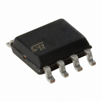
VIPER12AS STMicroelectronics, VIPER12AS Datasheet

VIPER12AS
Specifications of VIPER12AS
Available stocks
Related parts for VIPER12AS
VIPER12AS Summary of contents
Page 1
... Automatic burst mode in low load condition. – Overvoltage protection in hiccup mode. ON/OFF 60kHz OSCILLATOR PWM S LATCH OVERTEMP DETECTOR BLANKING OVERVOLTAGE LATCH VIPer12ADIP VIPer12AS SO-8 DIP-8 ORDER CODES TUBE T&R 13TR VIPer12AS VIPer12AS VIPer12ADIP DD DRAIN + _ 0.23 V 230 1 k SOURCE pin 1/15 ...
Page 2
... VIPer12ADIP / VIPer12AS PIN FUNCTION Name Power supply of the control circuits. Also provides a charging current during start up thanks to a high voltage current source connected to the drain. For this purpose, an hysteresis comparator monitors the V voltage and provides two thresholds Voltage value (typically 14.5V) at which the device starts switching and turns off the start up ...
Page 3
... D I =0.2A; T =100° =0.1A; V =300V (See fig. (See note 1) I =0.2A; V =300V (See fig. (See note 1) V =25V DS VIPer12ADIP / VIPer12AS Value Unit -0.3 ... 730 V -0.3 ... 400 V Internally limited A 0 ... 200 V 1.5 kV Internally limited C -40 to 150 C -55 to 150 C voltage has reached V ...
Page 4
... VIPer12ADIP / VIPer12AS ELECTRICAL CHARACTERISTICS (T SUPPLY SECTION Symbol Parameter Start Up Charging I DDch Current Start Up Charging I Current DDoff in Thermal Shutdown Operating Supply Current I DD0 Not Switching Operating Supply Current I DD1 Switching D Restart Duty Cycle RST V Undervoltage DD V DDoff Shutdown Threshold V V Start Up Threshold ...
Page 5
... Figure 1 : Rise and Fall Time 90 10% Figure 2 : Start Up VDD Current DD0 V DDhyst V V DDoff DDon I DDch Figure 3 : Restart Duty Cycle DDon V DDoff ------------------------ - RST << Coss t VDD FB CONTROL t rv VIPer12A 100 kHz VIPer12ADIP / VIPer12AS DRAIN 300V SOURCE VDD DRAIN FB CONTROL 100V SOURCE VIPer12A 5/15 ...
Page 6
... VIPer12ADIP / VIPer12AS Figure 4 : Peak Drain Current Vs. Feedback Current Dpeak 1/F OSC I FBsd The drain current limitation is obtained for VFB = 0 V, and a negative current is drawn from the FB pin. See the Application section for further details. Figure 5 : Thermal Shutdown HYST DDon 6/15 t 18V ...
Page 7
... Figure 6 : Switching Frequency vs Temperature 1.01 1 0.99 0.98 0.97 -20 Figure 7 : Current Limitation vs Temperature 1.04 1.03 1.02 1.01 1 0.99 0.98 0.97 0.96 0.95 0.94 -20 Vdd = 10V ... 35V Temperature (°C) Vin = 100V Vdd = 20V Temperature (°C) VIPer12ADIP / VIPer12AS 100 120 100 120 7/15 ...
Page 8
... VIPer12ADIP / VIPer12AS Figure 8 : Rectangular U-I output characteristics for battery charger RECTANGULAR U-I OUTPUT CHARACTERISTIC A complete regulation scheme can achieve combined and accurate output characteristics. Figure 8 presents a secondary feedback through an optocoupler driven by a TSM101. This device offers two operational amplifiers and a voltage reference, thus allowing the regulation of both output voltage and current ...
Page 9
... S PWM Q LATCH R Figure ONmin SOURCE -------------------------------------- - L 50mA t V ONmin -------------------------------------- - L VIPer12ADIP / VIPer12AS < where I FB FBsd FBsd FB FBsd and I as shown on figure 10 lower than V DD DDon , the start up current source is DDon Transfer function FB I Dpeak I ...
Page 10
... VIPer12ADIP / VIPer12AS Figure 11 : Start Up Sequence DDon V DDoff tss OUT the regulation point where the secondary loop begins to send a current in the optocoupler. At this point, the converter enters a regulated operation where the FB pin receives the amount of current needed to deliver the right power on secondary side ...
Page 11
... TYP 0.65 b 0.35 b1 0. 4.8 5 1.27 e3 3.81 F 3 0.8 VIPer12ADIP / VIPer12AS inch MAX. MIN. TYP. 1.75 0.25 0.003 1.65 0.85 0.025 0.48 0.013 0.25 0.007 0.5 0.010 45 (typ.) 5 0.188 6.2 0.228 0.050 0.150 4 0.14 1.27 0.015 0.6 8 (max.) 1 ...
Page 12
... VIPer12ADIP / VIPer12AS Plastic DIP-8 MECHANICAL DATA DIM Package Weight 12/15 mm. MIN. TYP 0.38 2.92 3.30 0.36 0.46 1.14 1.52 0.20 0.25 9.02 9.27 7.62 7.87 6.10 6.35 2.54 7.62 2.92 3.30 Gr. 470 MAX. 5.33 4.95 0.56 1.78 0.36 10.16 8.26 7.11 10 ...
Page 13
... All dimensions are in mm 1.5 1.5 5.5 4.5 2 End Top No components cover 500mm min tape Empty components pockets saled with cover tape. User direction of feed VIPer12ADIP / VIPer12AS 100 2000 532 3.2 6 0.6 2500 2500 330 1.5 13 20.2 12.4 60 18.4 Start Components ...
Page 14
... VIPer12ADIP / VIPer12AS A 14/15 DIP-8 TUBE SHIPMENT (no suffix) C Base Q.ty Bulk Q.ty Tube length (± 0. (± 0.1) All dimensions are in mm. 20 1000 532 8.4 11.2 0 ...
Page 15
... STMicroelectronics - Printed in ITALY- All Rights Reserved. Australia - Brazil - Canada - China - Finland - France - Germany - Hong Kong - India - Israel - Italy - Japan - Malaysia - Malta - Morocco - Singapore - Spain - Sweden - Switzerland - United Kingdom - U.S.A. The ST logo is a trademark of STMicroelectronics STMicroelectronics GROUP OF COMPANIES http://www.st.com VIPer12ADIP / VIPer12AS 15/15 ...


