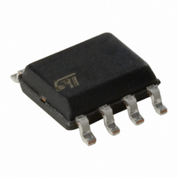
E-L6565D STMicroelectronics, E-L6565D Datasheet

E-L6565D
Specifications of E-L6565D
Related parts for E-L6565D
E-L6565D Summary of contents
Page 1
... R2 2.1V 1.6V January 2003 QUASI-RESONANT SMPS CONTROLLER DESCRIPTION The L6565 is a current-mode primary controller IC, specifically designed to build offline Quasi-resonant ZVS (Zero Voltage Switching at switch turn-on) fly- back converters. Quasi-resonant operation is achieved by means of a transformer demagnetization sensing input that trig- gers MOSFET's turn-on. ...
Page 2
... Blue Angel and Energy Star com- pliant. The IC includes also a disable function, an on-chip filter on current sense, an error amplifier with a precise ref- erence voltage for primary regulation and an effective two-level overcurrent protection. ...
Page 3
... THERMAL DATA Symbol R Max. Thermal Resistance, Junction-to-ambient th j-amb ABSOLUTE MAXIMUM RATINGS Symbol Pin Vcc Output Totem Pole Peak Current (2 µs) GD INV, COMP Analog Inputs & Outputs VFF Zero Current Detector ZCD P Power Dissipation @T tot T Junction Temperature Operating range j T Storage Temperature ...
Page 4
... START GATE DRIVER V Dropout Voltage Current Fall Time f t Current Rise Time sink current GDoff GD (1) Parameters guaranteed by design, not tested in production. 4/17 = 1nF; unless otherwise specified) o Test Condition Open loop 2.4 V COMP INV 2.6 V COMP INV I = 0.5 mA SOURCE ...
Page 5
... V 4.0 V 0.5 3 1nF 3 70KHz TA = 25°C V COMP (V) CC Figure 5. Pin 2 (COMP) V-I characteristics V [V] COMP 100 125 Figure 6. ZCD blanking time vs. COMP voltage D94IN048A T BLANK (°C) 100 = 2.5V 0.5 1 1.5 2 2.5 V [V] VFF °C Vpin1 = 0 Regulation range [mA] COMP [µ °C ...
Page 6
... Vcc - 0.5 -2.5 0 100 200 I [mA] GD Figure 9. IC consumption vs. temperature Icc [mA 0.5 0.2 0.1 0.05 0.02 - [°C] 6/17 Figure 10. Zener voltage at Vcc pin vs [ -50 400 500 Figure 11. Start-up timer period vs START 450 °C Vcc = 14.5 V SOURCE 400 350 300 250 300 400 ...
Page 7
... Quasi-resonant operation in offline flyback converters lies in synchronizing MOSFET's turn-on to the transform- er's demagnetization. Detecting the resulting negative-going edge of the voltage across any winding of the transformer can do this. The L6565 is provided with a dedicated pin that allows doing the job with a very simple interface, just one resistor. ...
Page 8
... Disable Block (see fig. 13): The ZCD pin is used also to activate the Disable Block. If the voltage on the pin is taken below 150 mV the de- vice will be shut down so necessary to override the source capability (10 mA max.) of the internal lower clamp ...
Page 9
... L6565 puts a limit on the minimum OFF-time of the switch. This is done by blanking the triggering block of the ZCD circuit as mentioned before. The duration of the blanking time (3.5µs min function of the error amplifier output VCOMP, as shown in the diagram of figure 6. If the load current and the input voltage are such that the switch OFF-time falls below the minimum blanking time of 3.5µ ...
Page 10
... The schematic in figure 17b shows also how the function is included in the control loop. With a proper selection of the external divider R1- possible to achieve the optimum compensation described by the lower curve in the diagram of figure 16 ...
Page 11
... A comparator senses the voltage on the current sense input and disables the gate driver if the voltage at the pin exceeds 2 V. Such anomalous condition is typically generated by a short circuit on the secondary rectifier or on the secondary winding. To re-enable the driver, first the IC must be turned off and then can be restarted, that is the Vcc voltage must fall below the UVLO threshold. ...
Page 12
... R12 47 k R13 C5 3.3 k 2.2 nF TRANSFORMER SPECS: CORE: ETD29x16x10, N67 material or equivalent 1 mm air gap for a primary inductance of 285 µH N1 (24T+24T series connected), 2xAWG28 ( N2 AWG28 N3 AWG28 Naux AWG32 ( Figure 20. 40W Wide Range Mains SMPS for inkjet printer 2A fuse 16R 1nF ...
Page 13
... APPLICATION IDEAS Here follows a series of ideas/suggestions aimed at either improving performance or solving common applica- tion issues of L6565-based power supplies. Figure 21. Enhanced turn-off for big MOSFET's drive Figure 22. Latched shutdown on: a) feedback disconnection; b) overload or short circuit BC327 a) Figure 23. Secondary Feedback loop configurations Vcc ...
Page 14
... BC327 1N4148 470 pF 2.7 k RELATED DOCUMENTATION [1] "L6565, QUASI-RESONANT CONTROLLER” (AN1326) [2] “25W QUASI-RESONANT FLYBACK CONVERTER FOR SET-TOP BOX APPLICATIONS USING THE L6565” (AN1376) [3] “EVAL6565N, 30W AC-DC ADAPTER WITH THE L6565 QUASI-RESONANT PWM CONTROLLER” (AN1439). 14/17 Vcc VFF E/A block ...
Page 15
... D 10.92 E 7.95 9.75 0.313 e 2.54 e3 7.62 e4 7.62 F 6.6 I 5.08 L 3.18 3.81 0.125 Z 1.52 inch TYP. MAX. 0.131 0.065 0.022 0.012 0.430 0.384 0.100 0.300 0.300 0.260 0.200 0.150 0.060 OUTLINE AND MECHANICAL DATA Minidip L6565 15/17 ...
Page 16
... F (1) 3.8 4.0 L 0.4 1.27 0.016 M 0 (max.) (1) D and F do not include mold flash or protrusions. Mold flash or potrusions shall not exceed 0.15mm (.006inch). 16/17 inch MIN. TYP. MAX. 0.069 0.010 0.065 0.033 0.019 0.010 0.020 0.197 0.244 ...
Page 17
... STMicroelectronics. The ST logo is a registered trademark of STMicroelectronics Australia - Brazil - Canada - China - Finland - France - Germany - Hong Kong - India - Israel - Italy - Japan -Malaysia - Malta - Morocco - Singapore - Spain - Sweden - Switzerland - United Kingdom - United States. ...


