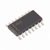
DS2715Z+ Maxim Integrated Products, DS2715Z+ Datasheet

DS2715Z+
Specifications of DS2715Z+
Related parts for DS2715Z+
DS2715Z+ Summary of contents
Page 1
... PIN CONFIGURATION C BIAS LED1 DNC V SS CTG CTG 16 SO See Table 1 for Ordering Information. Table 1. ORDERING INFORMATION PART MARKING DS2715Z+ D2715 DS2715Z+T&R D2715 DS2715BZ+ D2715B DS2715BZ+T&R D2715B + Denotes a lead(Pb)-free/RoHS-compliant package. T&R = Tape and reel. OPERATIONAL DIAGRAM DS2715 V BATT THM SNS- SNS+ ...
Page 2
ABSOLUTE MAXIMUM RATINGS* Voltage on V and V Pins with Respect Voltage on LED1 Pin Voltage on SNS- Voltage on C BIAS Voltage on all Other Pins Continuous Sink Current V CH Operating Temperature Range Storage ...
Page 3
PARAMETER SYMBOL Current Sense G Comparator Gain AC ELECTRICAL CHARACTERISTICS PARAMETER SYMBOL UVLO Debounce Time Current Sense Comparator Propagation Delay Discharge Detect Propagation Delay Return To Normal Function (Op-Amp or Comparator Mode) R Timing Accuracy T Internal Clock Accuracy ELECTRICAL ...
Page 4
PARAMETER SYMBOL dT/dt Blanking Time t PRECHARGE Timeout FAST-CHARGE Timer Range TOPOFF to FAST- CHARGE Duration Ratio Voltages relative to V Note 1: SS Does not include current through V Note 2: Below this voltage no I/O pins are active. ...
Page 5
Figure 1. BLOCK DIAGRAM ...
Page 6
Figure 2. STATE DIAGRAM ...
Page 7
DETAILED DESCRIPTION Charge Cycle Overview The DS2715 regulates the charge NiMH cells in a series configuration. With the mode select pin, the DS2715 can be configured to regulate either as an error amplifier in linear mode ...
Page 8
PRESENCE The DS2715 enters the PRESENCE state whenever V source is present, but no cell is available to charge. The DS2715 will remain in the PRESENCE state until a cell is inserted into the circuit causing the voltage on V ...
Page 9
Suspension of charge activity is possible by floating the R presence test conditions when suspending from a charge mode. The DISCHARGE mode is not affected by the SUSPEND function. The Vch output is high-impedance for charging modes, and operates as ...
Page 10
Hysteresis on the comparator input provides the difference between the ON and OFF state thresholds closed-loop regulation circuit, the comparator regulates voltage across the sense resistor as referenced to the SNS ...
Page 11
Figure 3. Ideal Comparator Input and Charge Control Output Waveforms sns Charge Rate Selection The charge rate is determined by an external sense resistor connected between the SNS+ and SNS- pins. The DS2715 will regulate the ...
Page 12
TEMPERATURE SENSE Accurate temperature sensing is needed to determine end of charge by dT/dt and to detect over temperature fault conditions. Connecting an external 10k NTC thermistor between THM and V Div and THM allows the DS2715 to sense temperature. ...
Page 13
Application Circuits Switchmode Figure 5 shows a typical DS2715 switchmode application circuit for charging a 3-cell battery stack. Connecting the MODE pin to CBIAS enables the comparator mode of current regulation. The DS2715 regulates the current through the current sense ...
Page 14
The R resistor (R5) is set to 47kΩ for a timeout of 70 minutes. This would be appropriate for cells with a capacity T of about 1Ah when charged with the 1.07A charge current. The resistor divider with R12 and ...
Page 15
Cell Stack Size Adjustment R12 and R13 of the application circuits form a voltage divider such that the voltage of a single cell is present on the Vbatt pin. This is required for proper operation of the DS2715. Given a ...
Page 16
Figure 7. Switching Circuit with Example Layout + Charge Source - Side - Charge Source Side + Another important layout detail is the connection of the sense resistor. Proper Kelvin connection layout should be used to ensure the signal quality ...
Page 17
REVISION HISTORY REVISION DATE 011408 Various comprehensive changes. 031609 Added device version DS2715B 042809 Updated Ordering Information table. DESCRIPTION PAGES CHANGED 6–15 1,4,7,8,10 1 ...


