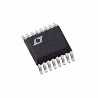
LTC4006EGN-2#TR Linear Technology, LTC4006EGN-2#TR Datasheet - Page 6

LTC4006EGN-2#TR
Manufacturer Part Number
LTC4006EGN-2#TR
Description
IC CHARGER BATTERY 4A 16-SSOP
Manufacturer
Linear Technology
Datasheet
1.LTC4006EGN-2PBF.pdf
(20 pages)
Specifications of LTC4006EGN-2#TR
Function
Charge Management
Battery Type
Lithium-Ion (Li-Ion)
Voltage - Supply
6 V ~ 28 V
Operating Temperature
-40°C ~ 85°C
Mounting Type
Surface Mount
Package / Case
16-SSOP (0.150", 3.90mm Width)
Output Current
4A
Output Voltage
12.6V
Operating Supply Voltage (min)
6V
Operating Supply Voltage (max)
28V
Operating Temp Range
-40C to 85C
Package Type
SSOP N
Mounting
Surface Mount
Pin Count
16
Operating Temperature Classification
Industrial
Lead Free Status / RoHS Status
Contains lead / RoHS non-compliant
Lead Free Status / RoHS Status
Contains lead / RoHS non-compliant
Available stocks
Company
Part Number
Manufacturer
Quantity
Price
R
placing a resistor, R
If this resistor is not present, the charger will not start.
GND (Pin 5): Ground for low power circuitry.
NTC (Pin 6): A thermistor network is connected from NTC
to GND. This pin determines if the battery temperature is
safe for charging. The charger and timer are suspended if
the thermistor indicates a temperature that is unsafe for
charging. The thermistor function may be disabled with a
300k to 500k resistor from DCIN to NTC.
I
Mode PWM. Higher I
charging currrent in normal operation. A 6.04k resistor, in
series with a capacitor of at least 0.1µF to GND, provides
loop compensation. Typical full-scale output current is
40µA. Nominal voltage range for this pin is 0V to 3V.
I
this pin provides a linear indication of charging current.
Peak current is equivalent to 1.19V. Zero current is ap-
proximately 0.309V. A capacitor from I
required to filter higher frequency components. If V
2.5V/cell, then V(I
depleted battery. Any current sourced or sinked from this
pin directly affects the charging current accuracy. If this
pin is to be monitored, a high impedance input buffer
should be used.
LTC4006
PI FU CTIO S
TEST CIRCUIT
6
TH
MON
T
The timer period is t
U
(Pin 7): Control Signal of the Inner Loop of the Current
(Pin 4): Timer Resistor. The timer period is set by
(Pin 8): Current Monitoring Output. The voltage at
U
MON
U
RT
TH
, to GND.
TIMER
) = 1.19V when conditioning a
voltage corresponds to higher
= (1hour • R
35mV
MON
RT
to ground is
/154k)
+
–
10
BAT
11.67µA
3k
BAT
<
9
CSP
V
CSP (Pin 9): Current Amplifier CA1 Input. This pin and the
BAT pin measure the voltage across the sense resistor,
R
quired for both peak and average current mode operation.
BAT (Pin 10): Battery Sense Input and the Negative
Reference for the Current Sense Resistor. A precision
internal resistor divider sets the final float potential on this
pin. The resistor divider is disconnected during shutdown.
CLP (Pin 11): Positive Input to the Supply Current Limiting
Amplifier, CL1. The threshold is set at 100mV above the
voltage at the CLN pin. When used to limit supply current,
a filter is needed to filter out the switching noise. If no
current limit function is desired, connect this pin to CLN.
CLN (Pin 12): Negative Reference for the Input Current
Limit Amplifier, CL1. This pin also serves as the power
supply for the IC. A 10µF to 22µF bypass capacitor should
be connected as close as possible to this pin.
TGATE (Pin 13): Drives the top external P-channel MOSFET
of the battery charger buck converter.
PGND (Pin 14): High Current Ground Return for the BGATE
Driver.
BGATE (Pin 15): Drives the bottom external N-channel
MOSFET of the battery charger buck converter.
INFET (Pin 16): Drives the Gate of the External Input PFET.
REF
SENSE
–
+
, to provide the instantaneous current signals re-
EA
LT1055
+
–
LTC4006
7
4006 TC
I
TH
0.6V
4006fa


