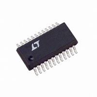
LTC4100EG#TR Linear Technology, LTC4100EG#TR Datasheet - Page 20

LTC4100EG#TR
Manufacturer Part Number
LTC4100EG#TR
Description
IC CHARGER SMART BATTERY 24-SSOP
Manufacturer
Linear Technology
Datasheet
1.LTC4100EGPBF.pdf
(30 pages)
Specifications of LTC4100EG#TR
Function
Charge Management
Battery Type
Smart Batteries
Voltage - Supply
6 V ~ 28 V
Operating Temperature
-40°C ~ 85°C
Mounting Type
Surface Mount
Package / Case
24-SSOP (0.200", 5.30mm Width)
Lead Free Status / RoHS Status
Contains lead / RoHS non-compliant
Available stocks
Company
Part Number
Manufacturer
Quantity
Price
LTC4100
OPERATION
The Current DAC Block
The current DAC is a delta-sigma modulator which controls
the effective value of an external resistor, R
set the current limit of the charger. Figure 7 is a simplifi ed
diagram of the DAC operation. The delta-sigma modulator
and switch convert the ChargingCurrent() value, received
via the SMBus, to a variable resistance equal to:
Therefore, programmed current is equal to:
When a value less than 1/16th of the maximum current
allowed by I
current DAC enters a different mode of operation called
LOWI. The current DAC output is pulse width modulated
with a high frequency clock having a duty cycle value of
1/8. Therefore, the maximum output current provided by
the charger is I
low duty cycle signal on and off. The delta-sigma shift
registers are then clocked at a slower rate, about 45ms/bit,
so that the charger has time to settle to the I
The resulting average charging current is equal to that
requested by the ChargingCurrent() value.
I
20
LIMIT
1.25R
I
for ChargingCurrent() < I
0
Figure 8. Charging Current Waveform in Low Current Mode
CHARGE
/8
SET
I
DC
= (102.3mV/R
20
/[ChargingCurrent()/I
~40ms
LIM
R
SET
Figure 7. Current DAC Operation
I
(FROM CA1 AMP)
MAX
PROG
is applied to the current DAC input, the
/8. The delta-sigma output gates this
V
REF
MODULATOR
SENSE
+
–
-
LIM[x]
) (ChargingCurrent()/I
AVERAGE CHARGER CURRENT
LIM[x]
.
CHARGING_CURRENT
VALUE
] = R
IDC
MAX
SET
4100 F07
, used to
/8 value.
19
LIM[x]
I
TH
),
4100 F08
Note: The LOWI mode can be disabled by setting the
NO_LOWI bit in the LTC0() function.
When wake-up is asserted to the current DAC block, the
delta-sigma is then fi xed at a value equal to 80mA, inde-
pendent of the I
Input FET
The input FET circuit performs two functions. It enables
the charger if the input voltage is higher than the CLP pin,
and provides an indication of this condition at both the
CHGEN pin and the PWR_FAIL bit in the ChargerStatus()
register. It also controls the gate of the input FET to keep
a low forward voltage drop when charging and prevents
reverse current fl ow through the input FET.
If the input voltage is less than V
130mV higher than V
pin is forced low unless this condition is met. The gate
of the input FET is driven to a voltage suffi cient to keep
a low forward voltage drop from drain to source. If the
voltage between DCIN and CLP drops to less than 25mV,
the input FET is turned off slowly. If the voltage between
DCIN and CLP is ever less than –25mV, then the input FET
is turned off quickly to prevent signifi cant reverse current
from fl owing in the input FET. In this condition the CHGEN
pin is driven low and the charger is disabled.
The AC Present Block (AC_PRESENT)
The DCDIV pin is used to determine AC presence. If the
DCDIV voltage is above the DCDIV comparator threshold
(V
and the AC_PRESENT bit in the ChargerStatus() func-
tion will be set. If the DCDIV voltage is below the DCDIV
comparator threshold minus the DCDIV comparator
hysteresis, then the ACP output pin is switched to GND
and the AC_PRESENT bit in the ChargerStatus() function
is cleared. The ACP output pin is designed to drive 2mA
continuously.
ACP
), then the ACP output pin will be switched to V
LIM
setting.
CLP
to activate the charger. The CHGEN
CLP
, it must go at least
4100fb
DD


