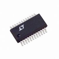
LTC4100EG#TR Linear Technology, LTC4100EG#TR Datasheet - Page 7

LTC4100EG#TR
Manufacturer Part Number
LTC4100EG#TR
Description
IC CHARGER SMART BATTERY 24-SSOP
Manufacturer
Linear Technology
Datasheet
1.LTC4100EGPBF.pdf
(30 pages)
Specifications of LTC4100EG#TR
Function
Charge Management
Battery Type
Smart Batteries
Voltage - Supply
6 V ~ 28 V
Operating Temperature
-40°C ~ 85°C
Mounting Type
Surface Mount
Package / Case
24-SSOP (0.200", 5.30mm Width)
Lead Free Status / RoHS Status
Contains lead / RoHS non-compliant
Available stocks
Company
Part Number
Manufacturer
Quantity
Price
TYPICAL PERFORMANCE CHARACTERISTICS
PIN FUNCTIONS
TGATE (Pin 1): Drives the Top External P-MOSFET of the
Battery Charger Buck Converter.
PGND (Pin 2): High Current Ground Return for BGATE
Driver.
BGATE (Pin 3): Drives the Bottom External N-MOSFET of
the Battery Charger Buck Converter.
INFET (Pin 4): Drives the Gate of the External Input
P-MOSFET.
DCIN (Pin 5): External DC Power Source Input. Bypass to
ground with a 0.1μF capacitor.
CHGEN (Pin 6): Digital Bidirectional Pin to Enable Charger
Function. This pin is connected as a wired AND bus.
The following events will cause the POWER_FAIL bit in
the ChargerStatus register to become set:
1. An external device pulling the CHGEN signal to within
2. The AC adapter voltage is not above the battery volt-
0.9V to GND;
age.
–0.1
–0.2
–0.3
–0.4
0.4
0.3
0.2
0.1
0
0
Charging Current Error
V
TEMP = 27°C
V
DD
LOAD
= 5V
= 12V
CHARGING CURRENT (A)
1
2
DCIN = 15V, NoLowI
DCIN = 20V, NoLowI
DCIN = 15V, LowI
DCIN = 20V, LowI
3
4100 G10
4
SMBALERT (Pin 7): Active Low Interrupt Output to Host
(referred to as the SMBALERT# signal in the SMBus Revi-
sion 1.1 specifi cation). Signals host that there has been a
change of status in the charger registers and that the host
should read the LTC4100 status registers to determine if
any action on its part is required. This signal can be con-
nected to the optional SMBALERT# line of the SMBus.
Open drain with weak current source pull-up to V
Schottky to allow it to be pulled to 5V externally).
SDA (Pin 8): SMBus Data Signal from Main (host-con-
trolled) SMBus. External pull-up resistor is required.
SCL (Pin 9): SMBus Clock Signal from Main (host-con-
trolled) SMBus. External pull-up resistor is required.
ACP (Pin 10): This Output Indicates the Value of the
DCDIV Comparator. It can be used to indicate whether
AC is present or not.
DCDIV (Pin 11): Supply Divider Input. This is a high im-
pedance comparator input with a 1.2V threshold (rising
edge) and hysteresis.
GND (Pin 12): Ground for Digital and Analog Circuitry.
–0.025
–0.050
–0.075
–0.100
–0.125
–0.150
0.150
0.125
0.100
0.075
0.050
0.025
0
0
Charging Voltage Error
V
TEMP = 27°C
I
LOAD
DD
2
= 5V
= 0.120A
4
CHARGING VOLTAGE (V)
6
8
DCIN = 15V
10
12
14
16
DCIN = 20V
18
20
4100 G11
22
LTC4100
DD
(with
4100fb
7


