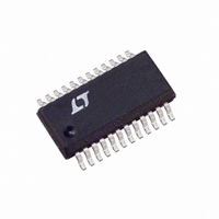
LTC4100EG#TRPBF Linear Technology, LTC4100EG#TRPBF Datasheet - Page 27

LTC4100EG#TRPBF
Manufacturer Part Number
LTC4100EG#TRPBF
Description
IC SMART BATTERY CHARGER 24-SSOP
Manufacturer
Linear Technology
Datasheet
1.LTC4100EGPBF.pdf
(30 pages)
Specifications of LTC4100EG#TRPBF
Function
Charge Management
Battery Type
Smart Batteries
Voltage - Supply
6 V ~ 28 V
Operating Temperature
-40°C ~ 85°C
Mounting Type
Surface Mount
Package / Case
24-SSOP (0.200", 5.30mm Width)
Lead Free Status / RoHS Status
Lead free / RoHS Compliant
Available stocks
Company
Part Number
Manufacturer
Quantity
Price
APPLICATIONS INFORMATION
PCB Layout Considerations
For maximum effi ciency, the switch node rise and fall times
should be minimized. To prevent magnetic and electrical fi eld
radiation and high frequency resonant problems, proper
layout of the components connected to the IC is essential.
(See Figure 11.) Here is a PCB layout priority list for proper
layout. Layout the PCB using this specifi c order.
1. Input capacitors need to be placed as close as possible
2. The control IC needs to be close to the switching FET’s
3. Place inductor input as close as possible to switching
to switching FET’s supply and ground connections.
Shortest copper trace connections possible. These
parts must be on the same layer of copper. Vias must
not be used to make this connection.
gate terminals. Keep the gate drive signals short for
a clean FET drive. This includes IC supply pins that
connect to the switching FET source pins. The IC can
be placed on the opposite side of the PCB relative to
above.
FET’s output connection. Minimize the surface area of
this trace. Make the trace width the minimum amount
needed to support current—no copper fi lls or pours.
Avoid running the connection using multiple layers in
parallel. Minimize capacitance from this node to any
other trace or plane.
4. Place the output current sense resistor right next to
5. Place output capacitors next to the sense resistor
6. Output capacitor ground connections need to feed
Interfacing with a Selector
The LTC4100 is designed to be used with a true analog
multiplexer for the SafetySignal sensing path. Some
selector ICs from various manufacturers may not imple-
ment this. Consult LTC applications department for more
information.
Electronic Loads
The LTC4100 is designed to work with a real battery.
Electronic loads will create instability within the LTC4100
preventing accurate programming currents and volt-
ages. Consult LTC applications department for more
information.
the inductor output but oriented such that the IC’s
current sense feedback traces going to resistor are not
long. The feedback traces need to be routed together
as a single pair on the same layer at any given time
with smallest trace spacing possible. Locate any fi lter
component on these traces next to the IC and not at
the sense resistor location.
output and ground.
into same copper that connects to the input capacitor
ground before tying back into system ground.
LTC4100
27
4100fb


