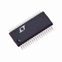
LTC1759CG#TRPBF Linear Technology, LTC1759CG#TRPBF Datasheet - Page 21

LTC1759CG#TRPBF
Manufacturer Part Number
LTC1759CG#TRPBF
Description
IC SMART BATTERY CHARGER 36SSOP
Manufacturer
Linear Technology
Datasheet
1.LTC1759CGPBF.pdf
(28 pages)
Specifications of LTC1759CG#TRPBF
Function
Charge Management
Battery Type
Smart Batteries
Voltage - Supply
11 V ~ 24 V
Operating Temperature
0°C ~ 70°C
Mounting Type
Surface Mount
Package / Case
36-SSOP (0.200", 5.30mm Width)
Lead Free Status / RoHS Status
Lead free / RoHS Compliant
Available stocks
Company
Part Number
Manufacturer
Quantity
Price
OPERATIO
Table 7. V
EXTERNAL
RESISTOR
(R
0
10k 1%
33k 1%
100k 1% 0.66V
Open or
Tied to V
The Voltage DAC Block
Note that the charge output voltage is offset by V
Therefore, the value of V
ChargingVoltage() value in order for the output voltage to
be programmed properly (without offset). If the
ChargingVoltage() value is below the nominal reference
voltage of the charger, nominally 2.465V, the charger
output voltage is programmed to zero. In addition, if the
ChargingVoltage() value is above the limit set by the V
pin, then the charger output voltage is set to the value
determined by the V
bit is set. These limits are demonstrated in Figure 6.
The Current DAC Block
The current DAC is a delta-sigma modulator which con-
trols the effective value of an external resistor, R
to set the current limit of the charger. Figure 7 is a
simplified diagram of the DAC operation. The delta-sigma
modulator and switch convert the ChargingCurrent() value,
received via the SMBus, to a variable resistance equal to:
Therefore, programmed current is equal to:
When a value less than 1/16th of the maximum current
allowed by I
current DAC enters a different mode of operation. The
current DAC output is pulse width modulated with a high
VLIMIT
0.8V
for ChargingCurrent() < I
1.25R
)
DD
REF
LIMIT
SET
V
0.17V
< 0.34V
0.42V
< 0.59V
< 0.84V
0.91V
V
/R
VLIMIT
LIMIT
LIMIT
/ChargingCurrent()/I
SET
Trip Points and Ranges
VDD
VCCP
VDD
VDD
VDD
VDD
VDD
VOLTAGE
< 0.09V
(ChargingCurrent()/I
< V
< V
< V
is applied to the current DAC input, the
U
< V
VLIMIT
VLIMIT
VLIMIT
VLIMIT
LIMIT
VCCP
REF
resistor and the VOLTAGE_OR
2465mV < V
< 8432mV
2465mV < V
< 12640mV
2465mV < V
< 16864mV
2465mV < V
< 21056mV
2465mV < V
< 32768mV
is subtracted from the SMBus
LIMIT[x]
VOLTAGE (V
CHARGING
NOMINAL
RANGE
LIMIT[x]
.
OUT
OUT
OUT
OUT
OUT
LIMIT
OUT
)
)
[x]),
GRANULARITY
16mV
16mV
32mV
32mV
32mV
SET
, used
LIMIT
REF
.
I
frequency clock having a duty cycle value of 1/8. There-
fore, the maximum output current provided by the charger
is I
signal on and off. The delta-sigma shift registers are then
clocked at a slower rate, about 45ms/bit, so that the
charger has time to settle to the I
average charging current is equal to that requested by the
ChargingCurrent() value.
LIMIT
0
Figure 8. Charging Current Waveform in Low Current Mode
MAX
/8
/8. The delta-sigma output gates this low duty cycle
~40ms
Figure 6. Transfer Function of Charger
NOTE: THE USER MUST ADJUST THE VALUE OF
THE EXTERNAL CURRENT SENSING COMPONENTS
(R
WITH I
R
25
20
15
10
SET
S1
PROG
5
0
I
SET
Figure 7. Current DAC Operation
, R
0
(FROM CA1 AMP)
LIMIT
S2
, R
5
I
SENSE
RANGES. SEE APPLICATIONS INFORMATION
PROG
V
REF
PROGRAMMED VALUE (V)
10
, R
MODULATOR
SET
+
–
15
) TO MAINTAIN CONSISTENCY
-
AVERAGE CHARGER CURRENT
20
MAX
25
/8 value. The resulting
30
CHARGINGCURRENT()
VALUE
TO
ERROR
AMP
LTC1759
35
1759 F06
1759 F07
21
1750 F08


