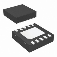
LM3658SDX/NOPB National Semiconductor, LM3658SDX/NOPB Datasheet - Page 5

LM3658SDX/NOPB
Manufacturer Part Number
LM3658SDX/NOPB
Description
IC USB/AC LI-ION CHARGER 10-LLP
Manufacturer
National Semiconductor
Type
Battery Chargerr
Datasheet
1.LM3658SD-ANOPB.pdf
(14 pages)
Specifications of LM3658SDX/NOPB
Function
Charge Management
Battery Type
Lithium-Ion (Li-Ion), Lithium-Polymer (Li-Pol)
Voltage - Supply
4.35 V ~ 6 V
Operating Temperature
-40°C ~ 85°C
Mounting Type
Surface Mount
Package / Case
10-WFDFN Exposed Pad
Output Current
25mA
Output Voltage
4.2V
Operating Supply Voltage (min)
4.35V
Operating Supply Voltage (max)
6V
Operating Temp Range
-40C to 85C
Package Type
LLP EP
Mounting
Surface Mount
Pin Count
10
Operating Temperature Classification
Industrial
For Use With
LM3658SDEV - BOARD EVALUATION LM3658SD
Lead Free Status / RoHS Status
Lead free / RoHS Compliant
Other names
LM3658SDX
Available stocks
Company
Part Number
Manufacturer
Quantity
Price
Company:
Part Number:
LM3658SDX/NOPB
Manufacturer:
TI
Quantity:
9 820
Part Number:
LM3658SDX/NOPB
Manufacturer:
TI/德州仪器
Quantity:
20 000
DETECTION AND TIMING
T
T
T
T
T
T
T
T
T
T
I/O
V
V
I
I
OL
OH
POK
PREQUAL
PQ_FULL
FULL_PQ
CHG
EOC
BATTEMP
DGL
ITOPOFF
TOPOFF
IL
IH
Symbol
Note 1: Absolute Maximum Ratings indicate limits beyond which damage to the component may occur. Operating Ratings are conditions under which operation
of the device is guaranteed. Operating Ratings do not imply guaranteed performance limits. For guaranteed performance limits and associated test conditions,
see the Electrical Characteristics tables.
Note 2: All voltages are with respect to the potential at the GND pin.
Note 3: The LM3658 has built-in thermal regulation to regulate the die temperature to 120ºC. See Operation Description section for more detail.
Note 4: The Human body model is a 100 pF capacitor discharged through a 1.5 kΩ resistor into each pin. The machine model is a 200 pF capacitor discharged
directly into each pin. MIL-STD-883 3015.7
Note 5: Junction-to-ambient thermal resistance is highly application and board-layout dependent. In applications where high maximum power dissipation exists,
special care must be paid to thermal dissipation issues in board design. Please refer to application note AN1187 for more detail.
Note 6: Min and Max limits are guaranteed by design, test, or statistical analysis. Typical numbers are not guaranteed, but do represent the most likely norm.
Note 7: LM3658 is not intended as a Li-Ion battery protection device; battery used in this application should have an adequate internal protection.
Power OK Deglitch
Time
Pre-Qualification Timer
Deglitch Time for Pre-
Qualification to Full-
Rate Charge Transition
Deglitch Time for Full-
Rate to Pre-
Qualification Transition
Charge Timer
Deglitch Time for End-
of-Charge Transition
Deglitch Time for
Battery Temperature
Fault
Deglitch Time for EN_b
and USB_sel Pins
Deglitch Time for
I
Top-Off Charging
Timer
Low-Level Input
Voltage
High-Level Input
Voltage
Low-Level Output
Current
High-Level Output
Current
TOPOFF
Parameter
V
LM3658SD, LM3658SD-B and LM3658SD-A
with USB_sel=high
LM3658SD-A with USB_sel=low
LM3658SD, LM3658SD-B and LM3658SD-A
with USB_sel=high
LM3658SD-A with USB_sel=low
EN_b
USB_sel
EN_b
USB_sel
STAT1, STAT2, output voltage = 0.25V
STAT1, STAT2, output voltage = 6.0V
BATT
< V
CC
– V
OK_CHG
Conditions
5
Min
270
270
270
540
270
270
1.4
2.5
40
27
20
20
27
54
10
0
0.01
Typ
300
300
300
600
300
300
60
30
40
40
30
60
25
Max
100
330
330
330
660
330
330
0.7
1.5
33
80
80
33
66
1
www.national.com
Units
mins
mins
mins
mA
ms
ms
ms
ms
ms
ms
ms
µA
V
V


