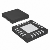
MAX8677CETG+T Maxim Integrated Products, MAX8677CETG+T Datasheet - Page 2

MAX8677CETG+T
Manufacturer Part Number
MAX8677CETG+T
Description
IC USB/AC ADP CHARGER 24-TQFN
Manufacturer
Maxim Integrated Products
Datasheet
1.MAX8677CETGT.pdf
(21 pages)
Specifications of MAX8677CETG+T
Function
Charge Management
Battery Type
Lithium-Ion (Li-Ion)
Voltage - Supply
4.1 V ~ 6.6 V
Operating Temperature
-40°C ~ 85°C
Mounting Type
Surface Mount
Package / Case
24-TQFN Exposed Pad
Lead Free Status / RoHS Status
Lead free / RoHS Compliant
ABSOLUTE MAXIMUM RATINGS
DC, PEN1 to GND .................................................-0.3V to +16V
USB to GND .............................................................-0.3V to +9V
VL to GND ................................................................-0.3V to +4V
BAT, SYS, CEN, USUS, PEN2, TSET to GND...........-0.3V to +6V
THM, PSET, ISET, CT to GND .........................-0.3V to VL + 0.3V
PREQ, CHG, DOK, UOK, FLT to GND .....................-0.3V to +6V
EP (exposed paddle) to GND ...............................-0.3V to +0.3V
DC Continuous Current (total in 2 pins) .........................2.4A
SYS Continuous Current (total in 2 pins) ........................2.4A
1.5A Dual-Input USB/AC Adapter Charger
and Smart Power Selector
Stresses beyond those listed under “Absolute Maximum Ratings” may cause permanent damage to the device. These are stress ratings only, and functional
operation of the device at these or any other conditions beyond those indicated in the operational sections of the specifications is not implied. Exposure to
absolute maximum rating conditions for extended periods may affect device reliability.
ELECTRICAL CHARACTERISTICS
(V
T
2
DC-TO-SYS PREREGULATOR
DC Operating Range
DC Standoff Voltage
DC Undervoltage Threshold
DC Overvoltage Threshold
DC Supply Current
DC Shutdown Current
DC-to-SYS On-Resistance
DC-to-BAT Dropout Voltage
DC Current Limit
(See Table 2 for Input Source
Control)
PSET Resistance Range
SYS Regulation Voltage
Input Current Soft-Start Time
Thermal-Limit Temperature
Thermal-Limit Gain
VL Voltage
A
DC
= -40°C to +85°C, unless otherwise noted. Typical values are at T
_______________________________________________________________________________________
= 5V, THM = CEN = USUS = GND, V
PARAMETER
V
W hen V
W hen V
I
I
V
I
When SYS regulation and charging stops, V
150mV hysteresis
V
T
V
Connecting DC when no USB present
Connecting DC with USB present
Die temperature at which charging and input current limits
are reduced
I
I
SYS
SYS
SYS
SYS
VL
A
BAT
DC
DC
DC
= +25°C
= 0 to 10mA
reduction/die temperature (above +100°C)
= I
= I
= V
= 400mA, V
= 6V, V
= 6V, I
= V
BAT
BAT
BAT
DOK
DOK
CEN
SYS
= 4V, V
SYS
= 0mA, V
= 0mA, V
SYS
g oes hi g h, V
g oes l ow , V
= USUS = 5V, V
= 0V
= 1mA to 1.75A, V
= 5V,
CEN
PEN1
CEN
CEN
= 5V
CONDITIONS
RMS
RMS
= V
D C
D C
= 0V
= 5V
PEN2
r i si ng , 500m V typ i cal hyster esi s
r i si ng , 360m V typ i cal hyster esi s
PEN1
R
R
R
V
(500mA USB mode)
V
(100mA USB mode)
= 5V, USB, TSET, PREQ, CHG, DOK, UOK, FLT are unconnected,
PEN1
PEN1
PSET
PSET
PSET
A
USB Continuous Current (total in 2 pins) .......................2.0A
BAT Continuous Current (total in 2 pins)........................2.4A
Continuous Power Dissipation (T
Operating Temperature Range ...........................-40°C to +85°C
Junction Temperature Range ............................-40°C to +125°C
Storage Temperature Range .............................-65°C to +150°C
Lead Temperature (soldering, 10s) .................................+300°C
CEN
= 0V
= +25°C.) (Note 1)
(derate 27.8mW/°C above +70°C) ........................... 2222mW
= 1.5kΩ
= 3kΩ
= 6.3kΩ
= 0V, V
= 0V, V
= 5V
DC
PEN2
PEN2
falling,
= 5V
= 0V
1800
3.95
4.29
MIN
900
450
450
4.1
6.8
1.5
3.0
10
80
A
= +70°C)
+100
2000
1000
TYP
4.35
195
475
475
4.0
6.9
0.8
0.2
1.5
3.3
50
95
50
1
5
MAX
2200
1100
4.05
0.35
4.40
333
500
500
100
6.6
7.0
1.5
6.3
3.6
14
90
2
UNITS
%/°C
mA
mV
mA
kΩ
ms
µA
°C
µs
Ω
V
V
V
V
V
V
RMS
RMS


