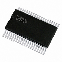
PCF8566T/1,118 NXP Semiconductors, PCF8566T/1,118 Datasheet - Page 15

PCF8566T/1,118
Manufacturer Part Number
PCF8566T/1,118
Description
IC LCD DVR UNVRSL LOW-MUX 40VSOP
Manufacturer
NXP Semiconductors
Datasheet
1.PCF8566T1118.pdf
(48 pages)
Specifications of PCF8566T/1,118
Package / Case
40-VSOP
Display Type
LCD
Configuration
7 Segment + DP, 14 Segment (24 Segment)
Interface
I²C
Current - Supply
30µA
Voltage - Supply
2.5 V ~ 6 V
Operating Temperature
-40°C ~ 85°C
Mounting Type
Surface Mount
Number Of Digits
12
Number Of Segments
96
Maximum Clock Frequency
315 KHz
Operating Supply Voltage
2.5 V to 6 V
Maximum Power Dissipation
400 mW
Maximum Operating Temperature
+ 85 C
Maximum Supply Current
90 uA
Minimum Operating Temperature
- 40 C
Lead Free Status / RoHS Status
Lead free / RoHS Compliant
Digits Or Characters
-
Lead Free Status / Rohs Status
Lead free / RoHS Compliant
Other names
568-1070-2
935278688118
PCF8566TD-T
935278688118
PCF8566TD-T
NXP Semiconductors
PCF8566_7
Product data sheet
7.5.1 Internal clock
7.5.2 External clock
7.5 Oscillator
7.6 Timing
The internal logic and the LCD drive signals of the PCF8566 are timed by the frequency
f
f
The clock frequency (f
for data reception from the I
rate of 100 kHz, f
The internal oscillator is enabled by connecting pin OSC to pin V
output from pin CLK is the clock signal for any cascaded PCF8566s or PCF8576s in the
system.
Connecting pin OSC to V
external clock input.
Remark: A clock signal must always be supplied to the device. Removing the clock,
freezes the LCD in a DC state.
The timing of the PCF8566 sequences the internal data flow of the device. This includes
the transfer of display data from the display RAM to the display segment outputs. In
cascaded applications, the synchronization signal (SYNC) maintains the correct timing
relationship between the PCF8566s in the system. The timing also generates the LCD
frame frequency which is derived as an integer division of the clock frequency (see
Table
used or by the frequency applied to the pin CLK when an external clock is used.
Table 6.
[1]
[2]
[3]
The ratio between the clock frequency and the LCD frame frequency depends on the
mode in which the device is operating. In the power-saving mode the reduction ratio is six
times smaller; this allows the clock frequency to be reduced by a factor of six. The
reduced clock frequency results in a significant reduction in power dissipation.
PCF8566 mode
normal mode
power saving mode
clk
clk(ext)
, which equals either the built-in oscillator frequency f
The possible values for f
For f
For f
6). The frame frequency is set by the mode set commands when an internal clock is
.
clk
clk
= 200 kHz.
= 31 kHz.
LCD frame frequencies
clk
should be chosen to be above 125 kHz.
Rev. 07 — 25 February 2009
clk
clk
) determines the LCD frame frequency (f
DD
see
2
enables an external clock source. Pin CLK then becomes the
C-bus. To allow I
Frame frequency
f
f
Table
fr
fr
=
=
[1]
20.
------------ -
2880
--------- -
480
f
f
clk
clk
Universal LCD driver for low multiplex rates
2
C-bus transmissions at their maximum data
osc
Nominal frame frequency (Hz)
69
65
or the external clock frequency
[2]
[3]
fr
SS
) and the maximum rate
. In this case, the
PCF8566
© NXP B.V. 2009. All rights reserved.
15 of 48


