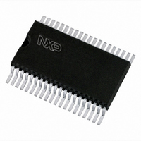
PCF8566T/1,118 NXP Semiconductors, PCF8566T/1,118 Datasheet - Page 17

PCF8566T/1,118
Manufacturer Part Number
PCF8566T/1,118
Description
IC LCD DVR UNVRSL LOW-MUX 40VSOP
Manufacturer
NXP Semiconductors
Datasheet
1.PCF8566T1118.pdf
(48 pages)
Specifications of PCF8566T/1,118
Package / Case
40-VSOP
Display Type
LCD
Configuration
7 Segment + DP, 14 Segment (24 Segment)
Interface
I²C
Current - Supply
30µA
Voltage - Supply
2.5 V ~ 6 V
Operating Temperature
-40°C ~ 85°C
Mounting Type
Surface Mount
Number Of Digits
12
Number Of Segments
96
Maximum Clock Frequency
315 KHz
Operating Supply Voltage
2.5 V to 6 V
Maximum Power Dissipation
400 mW
Maximum Operating Temperature
+ 85 C
Maximum Supply Current
90 uA
Minimum Operating Temperature
- 40 C
Lead Free Status / RoHS Status
Lead free / RoHS Compliant
Digits Or Characters
-
Lead Free Status / Rohs Status
Lead free / RoHS Compliant
Other names
568-1070-2
935278688118
PCF8566TD-T
935278688118
PCF8566TD-T
NXP Semiconductors
PCF8566_7
Product data sheet
7.12 Data pointer
When display data is transmitted to the PCF8566 the display bytes received are stored in
the display RAM based on the selected LCD drive mode. An example of a 7-segment
numeric display illustrating the storage order for all drive modes is shown in
The RAM storage organization applies equally to other LCD types.
The following applies to
The addressing mechanism for the display RAM is realized using the data pointer. This
allows the loading of an individual display data byte or a series of display data bytes, into
any location of the display RAM. The sequence commences with the initialization of the
data pointer by the load data pointer command (see
stored starting at the display RAM address indicated by the data pointer (see
Once each byte is stored, the data pointer is automatically incremented based on the
selected LCD configuration.
The contents of the data pointer are incremented as follows:
If an I
Consequently, the data pointer must be rewritten prior to further RAM accesses.
Fig 10. Display RAM bit map showing the direct relationship between display RAM
•
•
•
•
•
•
•
•
Static drive mode: the eight transmitted data bits are placed in row 0 to eight
successive display RAM addresses.
1:2 multiplex drive mode: the eight transmitted data bits are placed in row 0 and 1 to
four successive display RAM addresses.
1:3 multiplex drive mode: the eight transmitted data bits are placed in row 0, 1 and 2 of
three successive addresses, with bit 2 of the third address left unchanged. This last bit
can, if necessary, be controlled by an additional transfer to this address but avoid
overriding adjacent data because always full bytes are transmitted.
1:4 multiplex drive mode: the eight transmitted data bits are placed in row 0, 1, 2 and
3 to two successive display RAM addresses.
In static drive mode by eight.
In 1:2 multiplex drive mode by four.
In 1:3 multiplex drive mode by three.
In 1:4 multiplex drive mode by two.
2
C-bus data access terminates early, the state of the data pointer is unknown.
backplane outputs
display RAM bits
addresses and segment outputs and between bits in a RAM word and backplane
outputs
(rows)/
(BP)
Rev. 07 — 25 February 2009
0
1
2
3
Figure
0
1
11:
2
display RAM addresses (columns)/segment outputs (S)
3
4
Universal LCD driver for low multiplex rates
Table
13). After this, the data byte is
19
20
PCF8566
© NXP B.V. 2009. All rights reserved.
21
22
Figure
mgg389
Figure
23
17 of 48
11.
11).


