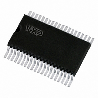
PCF8566T/1,118 NXP Semiconductors, PCF8566T/1,118 Datasheet - Page 21

PCF8566T/1,118
Manufacturer Part Number
PCF8566T/1,118
Description
IC LCD DVR UNVRSL LOW-MUX 40VSOP
Manufacturer
NXP Semiconductors
Datasheet
1.PCF8566T1118.pdf
(48 pages)
Specifications of PCF8566T/1,118
Package / Case
40-VSOP
Display Type
LCD
Configuration
7 Segment + DP, 14 Segment (24 Segment)
Interface
I²C
Current - Supply
30µA
Voltage - Supply
2.5 V ~ 6 V
Operating Temperature
-40°C ~ 85°C
Mounting Type
Surface Mount
Number Of Digits
12
Number Of Segments
96
Maximum Clock Frequency
315 KHz
Operating Supply Voltage
2.5 V to 6 V
Maximum Power Dissipation
400 mW
Maximum Operating Temperature
+ 85 C
Maximum Supply Current
90 uA
Minimum Operating Temperature
- 40 C
Lead Free Status / RoHS Status
Lead free / RoHS Compliant
Digits Or Characters
-
Lead Free Status / Rohs Status
Lead free / RoHS Compliant
Other names
568-1070-2
935278688118
PCF8566TD-T
935278688118
PCF8566TD-T
NXP Semiconductors
PCF8566_7
Product data sheet
8.1.1.1 START and STOP conditions
8.1.2 System configuration
8.1.3 Acknowledge
Both data and clock lines remain HIGH when the bus is not busy. A HIGH-to-LOW change
of the data line, while the clock is HIGH, is defined as the START condition (S).
A LOW-to-HIGH change of the data line, while the clock is HIGH, is defined as the STOP
condition (P). The START and STOP conditions are illustrated in
A device generating a message is a transmitter and a device receiving a message is the
receiver. The device that controls the message is the master and the devices which are
controlled by the master are the slaves. The system configuration is illustrated in
Figure
The number of data bytes transferred between the START and STOP conditions from
transmitter to receiver is unlimited. Each byte of eight bits is followed by an acknowledge
bit. The acknowledge bit is a HIGH level signal put on the bus by the transmitter during
which time the master generates an extra acknowledge related clock pulse. (See
Figure
Acknowledgement on the I
Fig 13. Definition of START and STOP conditions
Fig 14. System configuration
•
•
•
A slave receiver which is addressed must generate an acknowledge after the
reception of each byte.
A master receiver must generate an acknowledge after the reception of each byte that
has been clocked out of the slave transmitter.
The device that acknowledges must pull-down the SDA line during the acknowledge
clock pulse, so that the SDA line is stable LOW during the HIGH period of the
acknowledge related clock pulse (set-up and hold times must be taken into
consideration).
SCL
SDA
SDA
SCL
14.
15).
TRANSMITTER/
RECEIVER
MASTER
START condition
S
Rev. 07 — 25 February 2009
2
RECEIVER
C-bus is illustrated in
SLAVE
TRANSMITTER/
RECEIVER
Universal LCD driver for low multiplex rates
SLAVE
TRANSMITTER
MASTER
STOP condition
Figure
P
PCF8566
TRANSMITTER/
© NXP B.V. 2009. All rights reserved.
13.
RECEIVER
MASTER
mbc622
mga807
SDA
SCL
21 of 48


