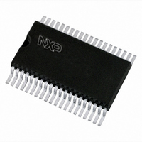
PCF8566T/1,118 NXP Semiconductors, PCF8566T/1,118 Datasheet - Page 24

PCF8566T/1,118
Manufacturer Part Number
PCF8566T/1,118
Description
IC LCD DVR UNVRSL LOW-MUX 40VSOP
Manufacturer
NXP Semiconductors
Datasheet
1.PCF8566T1118.pdf
(48 pages)
Specifications of PCF8566T/1,118
Package / Case
40-VSOP
Display Type
LCD
Configuration
7 Segment + DP, 14 Segment (24 Segment)
Interface
I²C
Current - Supply
30µA
Voltage - Supply
2.5 V ~ 6 V
Operating Temperature
-40°C ~ 85°C
Mounting Type
Surface Mount
Number Of Digits
12
Number Of Segments
96
Maximum Clock Frequency
315 KHz
Operating Supply Voltage
2.5 V to 6 V
Maximum Power Dissipation
400 mW
Maximum Operating Temperature
+ 85 C
Maximum Supply Current
90 uA
Minimum Operating Temperature
- 40 C
Lead Free Status / RoHS Status
Lead free / RoHS Compliant
Digits Or Characters
-
Lead Free Status / Rohs Status
Lead free / RoHS Compliant
Other names
568-1070-2
935278688118
PCF8566TD-T
935278688118
PCF8566TD-T
NXP Semiconductors
Table 8.
PCF8566_7
Product data sheet
Command
Mode set
Load data
pointer
Device select
Bank select
Blink
Definition of PCF8566 commands
Opcode
Bit 7 Bit 6 Bit 5 Bit 4 Bit 3 Bit 2 Bit 1 Bit 0
C
C
C
C
C
8.3.1 Mode set command
8.3 Command decoder
1
0
1
1
1
The command decoder identifies command bytes that arrive on the I
commands carry a continuation bit C in their most significant bit position as shown in
Figure
also represent a command. If this bit is reset, it indicates that the command byte is the last
in the transfer. Further bytes will be regarded as display data.
The five commands available to the PCF8566 are defined in
Table 9.
LCD drive mode
Drive mode
static
1:2
1:3
1:4
Fig 18. General format of byte command
0
0
1
1
1
(1) C = 0; last command.
(2) C = 1; commands continue.
18. When this bit is set, it indicates that the next byte of the transfer to arrive will
LP
P4
0
1
1
LCD drive mode command bit description
E
P3
0
1
0
Backplane
BP0
BP0, BP1
BP0, BP1. BP2
BP0, BP1. BP2, BP3
Rev. 07 — 25 February 2009
B
P2
A2
0
A
MSB
M1
P1
A1
I
BF1
C
M0
P0
A0
O
BF0
REST OF OPCODE
Reference
Section 8.3.1
Section 8.3.2
Section 8.3.3
Section 8.3.4
Section 8.3.5
Universal LCD driver for low multiplex rates
Bit
M1
0
1
1
0
msa833
Description
defines LCD drive mode, LCD bias
configuration, display status and
power dissipation mode
data pointer to define one of 24
display RAM addresses
define one of eight hardware
subaddresses
bit I: defines input bank selection
(storage of arriving display data);
bit O: defines output bank selection
(retrieval of LCD display data)
defines the blink frequency and blink
mode
LSB
Table
8.
M0
1
0
1
0
2
C-bus. All available
PCF8566
© NXP B.V. 2009. All rights reserved.
24 of 48


