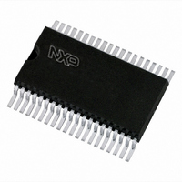
PCF8566T/1,118 NXP Semiconductors, PCF8566T/1,118 Datasheet - Page 43

PCF8566T/1,118
Manufacturer Part Number
PCF8566T/1,118
Description
IC LCD DVR UNVRSL LOW-MUX 40VSOP
Manufacturer
NXP Semiconductors
Datasheet
1.PCF8566T1118.pdf
(48 pages)
Specifications of PCF8566T/1,118
Package / Case
40-VSOP
Display Type
LCD
Configuration
7 Segment + DP, 14 Segment (24 Segment)
Interface
I²C
Current - Supply
30µA
Voltage - Supply
2.5 V ~ 6 V
Operating Temperature
-40°C ~ 85°C
Mounting Type
Surface Mount
Number Of Digits
12
Number Of Segments
96
Maximum Clock Frequency
315 KHz
Operating Supply Voltage
2.5 V to 6 V
Maximum Power Dissipation
400 mW
Maximum Operating Temperature
+ 85 C
Maximum Supply Current
90 uA
Minimum Operating Temperature
- 40 C
Lead Free Status / RoHS Status
Lead free / RoHS Compliant
Digits Or Characters
-
Lead Free Status / Rohs Status
Lead free / RoHS Compliant
Other names
568-1070-2
935278688118
PCF8566TD-T
935278688118
PCF8566TD-T
NXP Semiconductors
18. Soldering of SMD packages
PCF8566_7
Product data sheet
18.1 Introduction to soldering
18.2 Wave and reflow soldering
Table 24.
This text provides a very brief insight into a complex technology. A more in-depth account
of soldering ICs can be found in Application Note AN10365 “Surface mount reflow
soldering description” .
Soldering is one of the most common methods through which packages are attached to
Printed Circuit Boards (PCBs), to form electrical circuits. The soldered joint provides both
the mechanical and the electrical connection. There is no single soldering method that is
ideal for all IC packages. Wave soldering is often preferred when through-hole and
Surface Mount Devices (SMDs) are mixed on one printed wiring board; however, it is not
suitable for fine pitch SMDs. Reflow soldering is ideal for the small pitches and high
densities that come with increased miniaturization.
Wave soldering is a joining technology in which the joints are made by solder coming from
a standing wave of liquid solder. The wave soldering process is suitable for the following:
Not all SMDs can be wave soldered. Packages with solder balls, and some leadless
packages which have solder lands underneath the body, cannot be wave soldered. Also,
leaded SMDs with leads having a pitch smaller than ~0.6 mm cannot be wave soldered,
due to an increased probability of bridging.
The reflow soldering process involves applying solder paste to a board, followed by
component placement and exposure to a temperature profile. Leaded packages,
packages with solder balls, and leadless packages are all reflow solderable.
Key characteristics in both wave and reflow soldering are:
Symbol
E
F
G
H
x
y
•
•
•
•
•
•
•
Through-hole components
Leaded or leadless SMDs, which are glued to the surface of the printed circuit board
Board specifications, including the board finish, solder masks and vias
Package footprints, including solder thieves and orientation
The moisture sensitivity level of the packages
Package placement
Inspection and repair
Tray dimensions
Description
tray width; x direction
tray width; y direction
cut corner to pocket 1,1 center
cut corner to pocket 1,1 center
number of pockets; x direction
number of pockets; y direction
Rev. 07 — 25 February 2009
…continued
Universal LCD driver for low multiplex rates
Value
50.8 mm
50.8 mm
5.47 mm
5.47 mm
10
10
PCF8566
© NXP B.V. 2009. All rights reserved.
43 of 48


