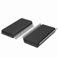
PCF85162T/1,118 NXP Semiconductors, PCF85162T/1,118 Datasheet - Page 15

PCF85162T/1,118
Manufacturer Part Number
PCF85162T/1,118
Description
IC LCD DISPLAY DVR 32SEG 48TSSOP
Manufacturer
NXP Semiconductors
Datasheet
1.PCF85162T1118.pdf
(43 pages)
Specifications of PCF85162T/1,118
Package / Case
48-TSSOP
Display Type
LCD
Configuration
32 Segment
Interface
I²C
Digits Or Characters
Any Digit Type
Current - Supply
8µA
Voltage - Supply
1.8 V ~ 5.5 V
Operating Temperature
-40°C ~ 85°C
Mounting Type
Surface Mount
Number Of Digits
16
Number Of Segments
128
Maximum Clock Frequency
400 KHz
Operating Supply Voltage
1.8 V to 5.5 V
Maximum Power Dissipation
400 mW
Maximum Operating Temperature
+ 85 C
Attached Touch Screen
No
Maximum Supply Current
50 mA
Minimum Operating Temperature
- 40 C
Dc
1123
Lead Free Status / RoHS Status
Lead free / RoHS Compliant
Other names
568-5059-2
NXP Semiconductors
PCF85162_2
Product data sheet
7.10 Display RAM
The display RAM is a static 32 × 4-bit RAM which stores LCD data. There is a one-to-one
correspondence between
A logic 1 in the RAM bitmap indicates the on-state of the corresponding LCD element;
similarly, a logic 0 indicates the off-state.
The display RAM bit map
backplane outputs BP0 to BP3, and the columns 0 to 31 which correspond with the
segment outputs S0 to S31. In multiplexed LCD applications the segment data of the first,
second, third, and fourth row of the display RAM are time-multiplexed with BP0, BP1,
BP2, and BP3 respectively.
When display data is transmitted to the PCF85162, the display bytes received are stored
in the display RAM in accordance with the selected LCD drive mode. The data is stored as
it arrives and does not wait for an acknowledge cycle as with the commands. Depending
on the current multiplex drive mode, data is stored singularly, in pairs, triples or
quadruples. To illustrate the filling order, an example of a 7-segment numeric display
showing all drive modes is given in
applies equally to other LCD types.
Fig 10. Display RAM bit map
•
•
•
•
In the static drive mode the same signal is carried by all four backplane outputs and
they can be connected in parallel for very high drive requirements.
the bits in the RAM bitmap and the LCD elements
the RAM columns and the segment outputs
the RAM rows and the backplane outputs.
display RAM rows/
backplane outputs
The display RAM bit map shows the direct relationship between the display RAM addresses and
the segment outputs and between the bits in a RAM word and the backplane outputs.
rows
(BP)
All information provided in this document is subject to legal disclaimers.
0
1
2
3
Rev. 02 — 7 May 2010
0
Figure 10
1
2
Figure
3
shows the rows 0 to 3 which correspond with the
display RAM addresses/segment outputs (S)
4
Universal LCD driver for low multiplex rates
11; the RAM filling organization depicted
columns
27
PCF85162
28
© NXP B.V. 2010. All rights reserved.
29
001aac265
30
31
15 of 43


