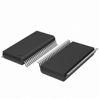
PCF85162T/1,118 NXP Semiconductors, PCF85162T/1,118 Datasheet - Page 19

PCF85162T/1,118
Manufacturer Part Number
PCF85162T/1,118
Description
IC LCD DISPLAY DVR 32SEG 48TSSOP
Manufacturer
NXP Semiconductors
Datasheet
1.PCF85162T1118.pdf
(43 pages)
Specifications of PCF85162T/1,118
Package / Case
48-TSSOP
Display Type
LCD
Configuration
32 Segment
Interface
I²C
Digits Or Characters
Any Digit Type
Current - Supply
8µA
Voltage - Supply
1.8 V ~ 5.5 V
Operating Temperature
-40°C ~ 85°C
Mounting Type
Surface Mount
Number Of Digits
16
Number Of Segments
128
Maximum Clock Frequency
400 KHz
Operating Supply Voltage
1.8 V to 5.5 V
Maximum Power Dissipation
400 mW
Maximum Operating Temperature
+ 85 C
Attached Touch Screen
No
Maximum Supply Current
50 mA
Minimum Operating Temperature
- 40 C
Dc
1123
Lead Free Status / RoHS Status
Lead free / RoHS Compliant
Other names
568-5059-2
NXP Semiconductors
PCF85162_2
Product data sheet
7.16.1 Bit transfer
7.16.2 START and STOP conditions
7.16 Characteristics of the I
Table 6.
[1]
The entire display can blink at a frequency other than the nominal blink frequency. This
can be effectively performed by resetting and setting the display enable bit E at the
required rate using the mode-set command (see
The I
The two lines are a Serial DAta line (SDA) and a Serial Clock Line (SCL). Both lines must
be connected to a positive supply via a pull-up resistor when connected to the output
stages of a device. Data transfer may be initiated only when the bus is not busy.
One data bit is transferred during each clock pulse. The data on the SDA line must remain
stable during the HIGH period of the clock pulse as changes in the data line at this time
will be interpreted as a control signal (see
Both data and clock lines remain HIGH when the bus is not busy.
A HIGH-to-LOW transition of the data line while the clock is HIGH is defined as the START
condition (S).
A LOW-to-HIGH transition of the data line while the clock is HIGH is defined as the STOP
condition (P) (see
Blink mode
off
1
2
3
Fig 12. Bit transfer
The blink frequency is proportional to the clock frequency (f
Table
2
C-bus is for bidirectional, two-line communication between different ICs or modules.
17.
Blink frequencies
All information provided in this document is subject to legal disclaimers.
SDA
SCL
Figure
Rev. 02 — 7 May 2010
13).
[1]
2
C-bus
data valid
data line
stable;
Figure
Universal LCD driver for low multiplex rates
Blink frequency equation
-
allowed
change
of data
f
f
f
blink
blink
blink
Table
12).
=
clk
=
=
). For the range of the clock frequency see
--------- -
768
------------ -
1536
f
------------ -
3072
clk
f
f
10).
clk
clk
mba607
PCF85162
© NXP B.V. 2010. All rights reserved.
19 of 43


