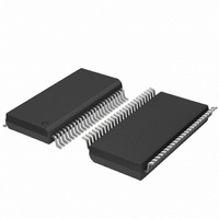
PCF85162T/1,118 NXP Semiconductors, PCF85162T/1,118 Datasheet - Page 21

PCF85162T/1,118
Manufacturer Part Number
PCF85162T/1,118
Description
IC LCD DISPLAY DVR 32SEG 48TSSOP
Manufacturer
NXP Semiconductors
Datasheet
1.PCF85162T1118.pdf
(43 pages)
Specifications of PCF85162T/1,118
Package / Case
48-TSSOP
Display Type
LCD
Configuration
32 Segment
Interface
I²C
Digits Or Characters
Any Digit Type
Current - Supply
8µA
Voltage - Supply
1.8 V ~ 5.5 V
Operating Temperature
-40°C ~ 85°C
Mounting Type
Surface Mount
Number Of Digits
16
Number Of Segments
128
Maximum Clock Frequency
400 KHz
Operating Supply Voltage
1.8 V to 5.5 V
Maximum Power Dissipation
400 mW
Maximum Operating Temperature
+ 85 C
Attached Touch Screen
No
Maximum Supply Current
50 mA
Minimum Operating Temperature
- 40 C
Dc
1123
Lead Free Status / RoHS Status
Lead free / RoHS Compliant
Other names
568-5059-2
NXP Semiconductors
PCF85162_2
Product data sheet
7.16.5 I
7.16.6 Input filters
7.16.7 I
The PCF85162 acts as an I
transmit data to an I
the acknowledge signals of the selected devices. Device selection depends on the
I
subaddress.
In single device applications, the hardware subaddress inputs A0, A1, and A2 are
normally tied to V
applications A0, A1, and A2 are tied to V
no two devices with a common I
subaddress.
To enhance noise immunity in electrical adverse environments, RC low-pass filters are
provided on the SDA and SCL lines.
Two I
PCF85162. The entire I
Table 7.
The PCF85162 is a write-only device and will not respond to a read access, therefore bit 0
should always be logic 0. Bit 1 of the slave address byte, that a PCF85162 will respond to,
is defined by the level tied to its SA0 input (V
Bit
2
2
2
Fig 15. Acknowledgement of the I
C-bus slave address, on the transferred command data and on the hardware
C-bus controller
C-bus protocol
2
C-bus slave addresses (0111 000 and 0111 001) are used to address the
by transmitter
data output
by receiver
data output
SCL from
Slave address
7
MSB
0
I
2
master
C slave address byte
All information provided in this document is subject to legal disclaimers.
SS
2
condition
6
1
which defines the hardware subaddress 0. In multiple device
C-bus master receiver. The only data output from the PCF85162 are
START
S
2
Rev. 02 — 7 May 2010
C-bus slave address byte is shown in
2
C-bus slave receiver. It does not initiate I
5
1
2
C-bus slave address have the same hardware
2
1
C-bus
4
1
SS
Universal LCD driver for low multiplex rates
or V
SS
2
DD
for logic 0 and V
3
0
using a binary coding scheme, so that
not acknowledge
2
0
acknowledge
Table
8
DD
for logic 1).
PCF85162
acknowledgement
7.
2
clock pulse for
1
SA0
C-bus transfers or
© NXP B.V. 2010. All rights reserved.
9
mbc602
0
LSB
R/W
21 of 43


