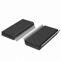
PCF85162T/1,118 NXP Semiconductors, PCF85162T/1,118 Datasheet - Page 22

PCF85162T/1,118
Manufacturer Part Number
PCF85162T/1,118
Description
IC LCD DISPLAY DVR 32SEG 48TSSOP
Manufacturer
NXP Semiconductors
Datasheet
1.PCF85162T1118.pdf
(43 pages)
Specifications of PCF85162T/1,118
Package / Case
48-TSSOP
Display Type
LCD
Configuration
32 Segment
Interface
I²C
Digits Or Characters
Any Digit Type
Current - Supply
8µA
Voltage - Supply
1.8 V ~ 5.5 V
Operating Temperature
-40°C ~ 85°C
Mounting Type
Surface Mount
Number Of Digits
16
Number Of Segments
128
Maximum Clock Frequency
400 KHz
Operating Supply Voltage
1.8 V to 5.5 V
Maximum Power Dissipation
400 mW
Maximum Operating Temperature
+ 85 C
Attached Touch Screen
No
Maximum Supply Current
50 mA
Minimum Operating Temperature
- 40 C
Dc
1123
Lead Free Status / RoHS Status
Lead free / RoHS Compliant
Other names
568-5059-2
NXP Semiconductors
PCF85162_2
Product data sheet
Having two reserved slave addresses allows the following on the same I
The I
condition (S) from the I
slave addresses available. All PCF85162 whose SA0 inputs correspond to bit 0 of the
slave address respond by asserting an acknowledge in parallel. This I
ignored by all PCF85162 whose SA0 inputs are set to the alternative level.
After an acknowledgement, one or more command bytes follow, that define the status of
each addressed PCF85162.
The last command byte sent is identified by resetting its most significant bit, continuation
bit C, (see
PCF85162s on the bus.
After the last command byte, one or more display data bytes may follow. Display data
bytes are stored in the display RAM at the address specified by the data pointer and the
subaddress counter. Both data pointer and subaddress counter are automatically updated
and the data directed to the intended PCF85162 device.
An acknowledgement after each byte is asserted only by the PCF85162 that are
addressed via address lines A0, A1, and A2. After the last display byte, the I
master asserts a STOP condition (P). Alternately a START may be asserted to restart an
I
2
Fig 16. I
Fig 17. Format of command byte
•
•
C-bus access.
Up to 16 PCF85162 for very large LCD applications
The use of two types of LCD multiplex drive modes
2
C-bus protocol is shown in
2
S
C-bus protocol
Figure
0 1 1 1 0 0
slave address
All information provided in this document is subject to legal disclaimers.
17). The command bytes are also acknowledged by all addressed
1 byte
2
C-bus master which is followed by one of two possible PCF85162
Rev. 02 — 7 May 2010
S
A
0
R/W
MSB
0 A C
C
Figure
acknowledge by
all addressed
n
PCF85162
COMMAND
≥ 1 byte(s)
REST OF OPCODE
16. The sequence is initiated with a START
Universal LCD driver for low multiplex rates
A
msa833
DISPLAY DATA
n
LSB
≥ 0 byte(s)
by A0, A1 and A2
update data pointers
subaddress counter
PCF85162 only
and if necessary,
acknowledge
PCF85162
selected
2
C-bus transfer is
© NXP B.V. 2010. All rights reserved.
A
2
C-bus:
013aaa235
P
2
C-bus
22 of 43


