MC14511BCPG ON Semiconductor, MC14511BCPG Datasheet
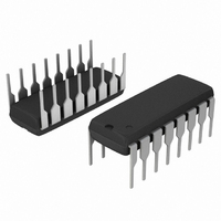
IC LATCH/DECODER/DRIVER 16DIP

MC14511BCPG

Manufacturer Part Number
MC14511BCPG
Description
IC LATCH/DECODER/DRIVER 16DIP
Manufacturer
ON Semiconductor
Datasheet

Specifications of MC14511BCPG

Configuration
7 Segment
Interface
BCD
Current - Supply
10µA
Voltage - Supply
3 V ~ 18 V
Operating Temperature
-55°C ~ 125°C
Mounting Type
Through Hole
Package / Case
16-DIP (0.300", 7.62mm)
Product
Decoder / Demultiplexer
Logic Family
MC14
Supply Voltage (max)
18 V
Supply Voltage (min)
3 V
Maximum Operating Temperature
+ 125 C
Minimum Operating Temperature
- 55 C
Mounting Style
Through Hole
Power Dissipation
500 mW
Lead Free Status / RoHS Status
Lead free / RoHS Compliant
Display Type
-
Digits Or Characters
-
Lead Free Status / Rohs Status
Lead free / RoHS Compliant
Other names
MC14511BCPGOS

Available stocks

Company
Part Number
Manufacturer
Quantity
Price
Part Number:
MC14511BCPG
Manufacturer:
ON/安森美
Quantity:
20 000
MC14511B
BCD-To-Seven Segment
Latch/Decoder/Driver
constructed with complementary MOS (CMOS) enhancement mode
devices and NPN bipolar output drivers in a single monolithic structure.
The circuit provides the functions of a 4−bit storage latch, an 8421
BCD−to−seven segment decoder, and an output drive capability. Lamp
test (LT), blanking (BI), and latch enable (LE) inputs are used to test the
display, to turn−off or pulse modulate the brightness of the display, and
to store a BCD code, respectively. It can be used with seven−segment
light−emitting diodes (LED), incandescent, fluorescent, gas discharge,
or liquid crystal readouts either directly or indirectly.
driver, computer/calculator display driver, cockpit display driver, and
various clock, watch, and timer uses.
Features
1. Maximum Ratings are those values beyond which damage to the device
2. Temperature Derating:
3. P
MAXIMUM RATINGS
© Semiconductor Components Industries, LLC, 2009
October, 2009 − Rev. 9
Symbol
P
I
The MC14511B BCD−to−seven segment latch/decoder/driver is
Applications include instrument (e.g., counter, DVM, etc.) display
OHmax
Schottky TTL Load, or Two HTL Loads Over the Rated Temperature
Range
Low Logic Circuit Power Dissipation
High−Current Sourcing Outputs (Up to 25 mA)
Latch Storage of Code
Blanking Input
Lamp Test Provision
Readout Blanking on all Illegal Input Combinations
Lamp Intensity Modulation Capability
Time Share (Multiplexing) Facility
Supply Voltage Range = 3.0 V to 18 V
Capable of Driving Two Low−power TTL Loads, One Low−power
Chip Complexity: 216 FETs or 54 Equivalent Gates
Triple Diode Protection on all Inputs
Pb−Free Packages are Available*
OHmax
V
T
may occur.
Plastic “P and D/DW” Packages: – 7.0 mW/°C From 65°C to 125°C
V
P
T
stg
DD
I
OHmax
in
D
A
= I
DC Supply Voltage Range
Input Voltage Range, All Inputs
DC Current Drain per Input Pin
Power Dissipation,
Operating Temperature Range
Storage Temperature Range
Maximum Output Drive Current
Maximum Continuous Output Power
OH
per Package (Note 2)
(Source) per Output
(Source) per Output (Note 3)
(V
DD
− V
(Voltages Referenced to V
Parameter
OH
)
SS
−0.5 to V
) (Note 1)
−0.5 to +18.0
−55 to +125
−65 to +150
Value
500
10
25
50
DD
+ 0.5
1
Unit
mW
mA
mA
mA
°C
°C
V
V
See detailed ordering and shipping information in the package
dimensions section on page 7 of this data sheet.
*For additional information on our Pb−Free strategy
and soldering details, please download the
ON Semiconductor Soldering and Mounting
Techniques Reference Manual, SOLDERRM/D.
ORDERING INFORMATION
A
WL, L
YY, Y
WW, W = Work Week
G
CASE 751B
DW SUFFIX
CASE 751G
SOEIAJ−16
CASE 648
CASE 966
D SUFFIX
P SUFFIX
F SUFFIX
http://onsemi.com
PDIP−16
SO−16
SO−16
= Assembly Location
= Wafer Lot
= Year
= Pb−Free Package
Publication Order Number:
16
1
MC14511BCP
AWLYYWWG
16
16
16
1
16
1
1
1
DIAGRAMS
AWLYYWWG
MARKING
MC14511B
AWLYWW
14511BG
MC14511B/D
14511B
ALYWG

Related parts for MC14511BCPG

MC14511BCPG Summary of contents

Page 1

... See detailed ordering and shipping information in the package 500 mW dimensions section on page 7 of this data sheet. −55 to +125 °C *For additional information on our Pb−Free strategy and soldering details, please download the −65 to +150 °C ON Semiconductor Soldering and Mounting Techniques Reference Manual, SOLDERRM/ http://onsemi.com MARKING DIAGRAMS ...

Page 2

This device contains protection circuitry to protect the inputs against damage due to high static voltages or electric fields. However advised that normal precautions be taken to avoid application of any voltage higher than maximum rated voltages to ...

Page 3

ELECTRICAL CHARACTERISTICS Î Î Î Î Î ...

Page 4

SWITCHING CHARACTERISTICS (Note 7) Î Î Î ...

Page 5

A, B, AND C ANY OUTPUT Figure 1. Dynamic Power Dissipation Signal Waveforms 20 ns 90% INPUT C 50% 10 PLH PHL 90% 50% OUTPUT g 10 TLH THL (a) Inputs D and LE low, and ...

Page 6

CONNECTIONS TO VARIOUS DISPLAY READOUTS INCANDESCENT READOUT GAS DISCHARGE READOUT filament pre−warm resistor is recommended to reduce filament thermal shock and increase the effective cold resistance ...

Page 7

... ORDERING INFORMATION Device MC14511BCP MC14511BCPG MC14511BD MC14511BDG MC14511BDR2G MC14511BDW MC14511BDWR2 MC14511BDWR2G MC14511BF MC14511BFG MC14511BFEL MC14511BFELG †For information on tape and reel specifications, including part orientation and tape sizes, please refer to our Tape and Reel Packaging Specifications Brochure, BRD8011/ PIN PIN 8 SS Figure 3. Logic Diagram Package PDIP− ...

Page 8

0.25 (0.010) −A− −T− SEATING PLANE 0.25 (0.010 PACKAGE DIMENSIONS PDIP−16 CASE 648−08 ...

Page 9

PACKAGE DIMENSIONS PLASTIC SOIC PACKAGE 16X 0. SEATING e PLANE 14X T SO− SUFFIX CASE 751G−03 ISSUE C NOTES DIMENSIONS ARE IN ...

Page 10

... Opportunity/Affirmative Action Employer. This literature is subject to all applicable copyright laws and is not for resale in any manner. PUBLICATION ORDERING INFORMATION LITERATURE FULFILLMENT: Literature Distribution Center for ON Semiconductor P.O. Box 5163, Denver, Colorado 80217 USA Phone: 303−675−2175 or 800−344−3860 Toll Free USA/Canada Fax: 303− ...

Related keywords