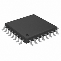
MAX1493CCJ+ Maxim Integrated Products, MAX1493CCJ+ Datasheet

MAX1493CCJ+
Specifications of MAX1493CCJ+
Related parts for MAX1493CCJ+
MAX1493CCJ+ Summary of contents
Page 1
... DIP MAX1493CCJ 0°C to +70°C 32 TQFP MAX1495CCJ 0°C to +70°C 32 TQFP ________________________________________________________________ Maxim Integrated Products For pricing, delivery, and ordering information, please contact Maxim/Dallas Direct! at 1-888-629-4642, or visit Maxim’s website at www.maxim-ic.com. 3.5- and 4.5-Digit, Single-Chip ADCs with LCD Drivers ♦ ...
Page 2
Single-Chip ADCs with LCD Drivers ABSOLUTE MAXIMUM RATINGS AV to GND............................................................-0. GND ...........................................................-0.3V to +6V DD AIN+, AIN- to GND...............................V REF+, REF- to GND..............................V LOWBATT to GND ...................................-0.3V to (AV INTREF, RANGE, ...
Page 3
ELECTRICAL CHARACTERISTICS (continued) ( +2.7V to +5.25V, GND = unless otherwise noted. Typical values are at +25°C, unless otherwise noted.) MAX PARAMETER SYMBOL LOW-BATTERY VOLTAGE MONITOR (LOWBATT) LOWBATT Trip Threshold ...
Page 4
Single-Chip ADCs with LCD Drivers ELECTRICAL CHARACTERISTICS (continued) ( +2.7V to +5.25V, GND = unless otherwise noted. Typical values are at +25°C, unless otherwise noted.) MAX PARAMETER ...
Page 5
DV = 5V, GND = 0, REF+ = 2.048V, REF- = GND, RANGE = MAX1493/MAX1495 (±200mV INPUT RANGE) INL vs. DISPLAY COUNT 1.0 0.5 0 -0.5 -1.0 -20,000 -10,000 0 10,000 20,000 DISPLAY COUNT SUPPLY ...
Page 6
Single-Chip ADCs with LCD Drivers ( 5V, GND = 0, REF+ = 2.048V, REF- = GND, RANGE = INTERNAL REFERENCE VOLTAGE vs. TEMPERATURE 2.054 2.053 2.052 2.051 2.050 2.049 2.048 2.047 ...
Page 7
PIN NAME MAX1493 MAX1491 MAX1495 Internal Reference Logic Input. Connect to GND to select external reference mode. Connect 1 30 INTREF to DV Digital Power Input. Connect with a 0.1µF and a 4.7µF capacitor. 3 ...
Page 8
Single-Chip ADCs with LCD Drivers PIN NAME MAX1493 MAX1491 MAX1495 21 18 SEG7 LCD Segment 7 Driver 22 19 SEG8 LCD Segment 8 Driver 23 20 SEG9 LCD Segment 9 Driver 24 21 SEG10 LCD Segment 10 ...
Page 9
Detailed Description The MAX1491/MAX1493/MAX1495 low-power, highly integrated ADCs with LCD drivers convert a ±2V differ- ential input voltage (one count is equal to 100µV for the MAX1493/MAX1495 and 1mV for the MAX1491) with a sigma-delta ADC and output the result ...
Page 10
Single-Chip ADCs with LCD Drivers The MAX1491/MAX1493/MAX1495 contain an internal oscillator. Using the internal oscillator saves board space by removing the need for an external clock source. The oscillator is optimized to give 50Hz and 60Hz power ...
Page 11
HOLD Figure 4. Backplane Connection for the MAX1493/MAX1495 (4.5 Digits) SEG13: PEAK, HOLD, N.C. HOLD SEG12: F4, E4, DP4 SEG11: A4, G4, D4 SEG10: B4, C4, BC5 SEG9: F3, E3, DP3 SEG8: A3, G3, D3 Figure 5. Segment Connection for ...
Page 12
Single-Chip ADCs with LCD Drivers HOLD Figure 6. Backplane Connection for the MAX1491 (3.5 Digits) SEG10: PEAK, HOLD, BC4 SEG9: F3, E3, DP3 SEG8: A3, G3, D3 Figure 7. Segment Connection for the MAX1491 (3.5 Digits) X ...
Page 13
BP1 BP2 BP3 ALL OFF OFF OFF OFF φ1, φ2, φ HIGH WITH RESPECT TO SEGMENT (BP+ TIME) φ1', φ2', φ LOW ...
Page 14
Single-Chip ADCs with LCD Drivers BP1 BP2 BP3 ALL OFF OFF OFF OFF φ1, φ2, φ HIGH WITH RESPECT TO SEGMENT (BP+ ...
Page 15
ALL OFF OFF OFF ALL VOLTAGE CONTRAST RATIO = V φ1, φ2, φ HIGH WITH RESPECT TO SEGMENT (BP+ TIME) φ1', φ2', ...
Page 16
Single-Chip ADCs with LCD Drivers 100 Figure 12. Contrast vs. Applied RMS Voltage 16 ______________________________________________________________________________________ Ø = -10°C Ø = +10°C Ø = -30°C Ø = 0°C V ...
Page 17
If ghosting is present on the LCD, the RMS OFF voltage is too high. Choose an LCD with a higher RMS OFF voltage or decrease Decimal Point Control The MAX1491/MAX1493/MAX1495 allow for full deci- mal-point control and ...
Page 18
Single-Chip ADCs with LCD Drivers offers enhanced offset calibration on demand. Connect HOLD to DV for 2s to perform enhanced offset cali- DD bration. The MAX1491/MAX1493/MAX1495 feature peak detec- tion circuitry. When activated (PEAK connected to DV ...
Page 19
Transfer Functions Figures 15–18 show the MAX1491/MAX1493s’ transfer functions. The transfer function for the MAX1493/ MAX1495 with AIN+ - AIN- ≥ 0 and RANGE = GND is: ⎛ AIN = × Counts 1 024 . ⎜ ...
Page 20
Single-Chip ADCs with LCD Drivers LCD 1999 -1999 - -100µV 100µV 0 -200mV ANALOG INPUT VOLTAGE Figure 17. MAX1491 Transfer ...
Page 21
Gain error is the amount of deviation between the mea- sured full-scale transition point and the ideal full-scale transition point. Common-Mode Rejection Common-mode rejection is the ability of a device to reject a signal that is common to both input ...
Page 22
Single-Chip ADCs with LCD Drivers Pin Configurations (continued) TOP VIEW INTREF GND AIN+ 5 MAX1491 AIN- 6 REF- 7 REF+ 8 LOWBATT 9 RANGE 10 DPSET1 11 DPSET2 12 ...
Page 23
For the latest package outline information go to www.maxim-ic.com/packages.) ______________________________________________________________________________________ 3.5- and 4.5-Digit, Single-Chip ADCs with LCD Drivers Package Information 23 ...
Page 24
Single-Chip ADCs with LCD Drivers (The package drawing(s) in this data sheet may not reflect the most current specifications. For the latest package outline information go to www.maxim-ic.com/packages NOTES: 1. D&E ...
Page 25
... Maxim cannot assume responsibility for use of any circuitry other than circuitry entirely embodied in a Maxim product. No circuit patent licenses are implied. Maxim reserves the right to change the circuitry and specifications without notice at any time. Maxim Integrated Products, 120 San Gabriel Drive, Sunnyvale, CA 94086 408-737-7600 ____________________ 25 © 2004 Maxim Integrated Products 3 ...


