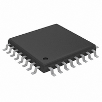
MAX1495CCJ+ Maxim Integrated Products, MAX1495CCJ+ Datasheet - Page 10

MAX1495CCJ+
Manufacturer Part Number
MAX1495CCJ+
Description
IC ADC 4.5 DGT LCD DVR 32-TQFP
Manufacturer
Maxim Integrated Products
Datasheet
1.MAX1491CAI.pdf
(25 pages)
Specifications of MAX1495CCJ+
Display Type
LCD
Configuration
7 Segment + 2 Annunciators
Digits Or Characters
A/D 4.5 Digits
Current - Supply
980µA
Voltage - Supply
2.7 V ~ 5.25 V
Operating Temperature
0°C ~ 70°C
Mounting Type
Surface Mount
Package / Case
32-LQFP
Maximum Operating Temperature
+ 70 C
Mounting Style
SMD/SMT
Minimum Operating Temperature
0 C
Lead Free Status / RoHS Status
Lead free / RoHS Compliant
Interface
-
Lead Free Status / Rohs Status
Lead free / RoHS Compliant
3.5- and 4.5-Digit, Single-Chip
ADCs with LCD Drivers
The MAX1491/MAX1493/MAX1495 contain an internal
oscillator. Using the internal oscillator saves board
space by removing the need for an external clock
source. The oscillator is optimized to give 50Hz and
60Hz power supply and common-mode rejection.
The MAX1491/MAX1493/MAX1495 contain an internal
charge pump to provide the negative supply voltage for
the internal analog input/reference buffers. The bipolar
input range of the analog input/reference buffers allows
the devices to accept negative inputs with high source
impedances. For the charge pump to operate correctly,
connect a 0.1µF capacitor from V NEG to GND.
The MAX1491/MAX1493/MAX1495 contain the neces-
sary backplane and segment driver outputs to drive
3.5-digit (MAX1491) and 4.5-digit (MAX1493/MAX1495)
LCDs. The LCD update rate is 2.5Hz. Figures 4–7 show
the connection schemes for a standard LCD. The
MAX1491/MAX1493/MAX1495 automatically display the
results of the ADC.
An internal resistor string of three equal-value resistors
(52kΩ, 1% matching) is used to generate the display
drive voltages. One end of the string is connected to
DV
V
threshold voltage for the liquid-crystal material used.
The connection diagram for a typical 7-segment display
font with two annunciators is illustrated in Figure 3 and
Figure 8. The MAX1491/MAX1493/MAX1495 numeric
display drivers (4.5 digits, 3.5 digits) use this configura-
tion to drive a triplexed LCD with three backplanes and
13 segment driver lines (10 for 3.5 digits). Figures 4 and
5 show the assignment of the 4.5-digit display segments
and Figures 6 and 7 show the assignment of the 3.5-
digit display segments.
The voltage waveforms of the backplane lines and y
segment line (Figure 3) have been chosen as an exam-
ple. This line intersects with BP1 to form the a segment,
Table 1. List of LCD Manufacturers
10
The following site has links to other custom LCD manufacturers: www.earthlcd.com/mfr.htm
LCD
MANUFACTURER
DD
______________________________________________________________________________________
DCI, Inc.
(V
and the other end is connected to GND. Note that
LCD
= DV
DD
www.dciincorporated.com
- GND) should be three times the
WEBSITE
Internal Clock
Charge Pump
LCD Driver
Triplexing
PART NUMBER
04-0924-00
04-0924-01
04-0925-00
04-0925-01
with BP2 to form the g segment, and with BP3 to form
the d segment. Eight different ON/OFF combinations of
the a, g, and d segments and their corresponding
waveforms of the y segment line are illustrated in
Figures 9 and 10. The schematic diagram in Figure 8
shows that each intersection acts as a capacitance
from segment line to common line. Figure 11 illustrates
the voltage across the g segment.
The RMS voltage across the segment determines the
degree of polarization for the liquid-crystal material and
thus the contrast of the segment. The RMS OFF voltage
is always V
always 1.92V
ratio of RMS ON to OFF voltage is fixed at 1.92 for a
triplexed LCD.
Figure 12 illustrates contrast vs. applied RMS voltage
with a V
the RMS OFF voltage is 1.1V. The OFF segment has a
contrast of less than 5%, while the ON segments have
greater than 85% contrast.
Figure 3. Connection Diagrams for Typical Seven-Segment
Displays
DP
X
e
LCD
f
d
g
LCD
a
of 3.1V. The RMS ON voltage is 2.1V and
LCD
Y
ANNUNCIATOR
/ 3, whereas the RMS ON voltage is
c
/ 3. This is illustrated in Figure 11. The
b
Z
BP1
BP2
BP3
DESCRIPTION
DP
3.5 digit, 5V
3.5 digit, 3V
4.5 digit, 5V
4.5 digit, 3V
e
f
d
g
a
ANNUNCIATOR
c
b


