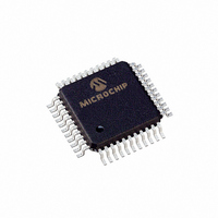
TC7129CKW Microchip Technology, TC7129CKW Datasheet - Page 15

TC7129CKW
Manufacturer Part Number
TC7129CKW
Description
IC ADC 4 1/2DGT LCD DVR 44-MQFP
Manufacturer
Microchip Technology
Datasheet
1.TC7129CPL.pdf
(28 pages)
Specifications of TC7129CKW
Display Type
LCD
Configuration
7 Segment
Digits Or Characters
A/D 4.5 Digits
Current - Supply
800µA
Voltage - Supply
6 V ~ 12 V
Operating Temperature
0°C ~ 70°C
Mounting Type
Surface Mount
Package / Case
44-MQFP, 44-PQFP
Lead Free Status / RoHS Status
Lead free / RoHS Compliant
Interface
-
Available stocks
Company
Part Number
Manufacturer
Quantity
Price
Company:
Part Number:
TC7129CKW
Manufacturer:
Microchip Technology
Quantity:
151
Company:
Part Number:
TC7129CKW
Manufacturer:
Microchip Technology
Quantity:
10 000
Company:
Part Number:
TC7129CKW713
Manufacturer:
MICROCHIP
Quantity:
12 000
Company:
Part Number:
TC7129CKW713
Manufacturer:
Microchip Technology
Quantity:
10 000
4.11
The integrator section includes the integrator, compar-
ator, input buffer amplifier and analog switches (see
Table 4-2) used to change the circuit configuration
during the separate measurement phases described
earlier. (See Figure 4-12).
TABLE 4-2:
The buffer amplifier has a common mode input voltage
range from 1.5V above V– to 1V below V+. The integra-
tor amplifier can swing to within 0.3V of the rails.
However, for best linearity, the swing is usually limited
to within 1V. Both amplifiers can supply up to 80 A of
output current, but should be limited to 20 A for good
linearity.
4.12
A comparator with a 200 mV threshold is connected
between IN HI (pin 33) and IN LO (pin 32). Whenever
the voltage between inputs is less than 200 mV, the
CONTINUITY output (pin 27) will be pulled high,
activating the continuity annunciator on the display.
The continuity pin can also be used as an input to drive
the continuity annunciator directly from an external
source (see Figure 4-13).
A schematic of the input/output nature of this pin is also
shown in Figure 4-14.
© 2006 Microchip Technology Inc.
Label
REST
Label
DE+
INT
INT
DE–
X10
X10
INT
DE
ZI
1
2
Integrator Section
Continuity Indicator
Meaning.
Open during all de-integrate phases.
input voltage is negative.
input voltage is positive.
Closed during the first integrate phase
(measurement of the input voltage).
Closed during the second integrate phase
(measurement of the amplifier offset).
Open during both integrate phases.
Closed during the rest phase.
Closed during the zero integrate phase.
Closed during the X10 phase.
Open during the X10 phase.
Closed during all de-integrate phases when
Closed during all de-integrate phases when
SWITCH LEGENDS
Description
Figure 4-13:
Figure 4-14:
4.13
The common and digital ground (DGND) outputs are
generated from internal Zener diodes. The voltage
between V+ and DGND is the internal supply voltage
for the digital section of the TC7129. Common can
source approximately 12 A; DGND has essentially no
source capability (see Figure 4-15).
CONT
IN LO
IN HI
COM
CONTINUITY, Pin 27
LATCH/HOLD Pin 22
DP
DP
Common and Digital Ground
4
3
/OR, Pin 20
/UR, Pin 21
200 mV
V
–
+
Continuity Indicator Circuit.
Input/Output Pin Schematic.
500 k
500 k
TC7129
TC7129
To Display Driver
DS21459D-page 15
(Not Latched)
TC7129
–
+
Buffer


