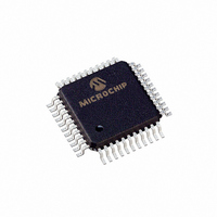
TC7129CKW Microchip Technology, TC7129CKW Datasheet - Page 3

TC7129CKW
Manufacturer Part Number
TC7129CKW
Description
IC ADC 4 1/2DGT LCD DVR 44-MQFP
Manufacturer
Microchip Technology
Datasheet
1.TC7129CPL.pdf
(28 pages)
Specifications of TC7129CKW
Display Type
LCD
Configuration
7 Segment
Digits Or Characters
A/D 4.5 Digits
Current - Supply
800µA
Voltage - Supply
6 V ~ 12 V
Operating Temperature
0°C ~ 70°C
Mounting Type
Surface Mount
Package / Case
44-MQFP, 44-PQFP
Lead Free Status / RoHS Status
Lead free / RoHS Compliant
Interface
-
Available stocks
Company
Part Number
Manufacturer
Quantity
Price
Company:
Part Number:
TC7129CKW
Manufacturer:
Microchip Technology
Quantity:
151
Company:
Part Number:
TC7129CKW
Manufacturer:
Microchip Technology
Quantity:
10 000
Company:
Part Number:
TC7129CKW713
Manufacturer:
MICROCHIP
Quantity:
12 000
Company:
Part Number:
TC7129CKW713
Manufacturer:
Microchip Technology
Quantity:
10 000
1.0
Absolute Maximum Ratings*
Supply Voltage (V+ to V-)....................................... 15V
Reference Voltage (REF HI or REF LO) ........ V+ to V–
Input Voltage (IN HI or IN LO) (Note 1).......... V+ to V–
V
Digital Input (Pins 1, 2, 19, 20,
Analog Input (Pins 25, 29, 30) ....................... V+ to V–
Package Power Dissipation (T
Operating Temperature Range ............... 0°C to +70°C
Storage Temperature Range.............. -65°C to +150°C
TC7129 ELECTRICAL SPECIFICATIONS
© 2006 Microchip Technology Inc.
Electrical Characteristics: V+ to V– = 9V, V
Pin numbers refer to 40-pin DIP.
Input
RE
NL
CMRR
CMVR
e
I
Note 1:
Symbol
DISP
IN
N
21, 22, 27, 37, 39, 40) .......................... DGND to V+
Plastic DIP ..................................................... 1.23W
PLCC ............................................................. 1.23W
Plastic QFP .................................................... 1.00W
.......................................... V+ to (DGND – 0.3V)
ELECTRICAL
CHARACTERISTICS
Zero Input Reading
Zero Reading Drift
Ratiometric Reading
Range Change Accuracy
Rollover Error
Linearity Error
Common Mode Rejection Ratio
Common Mode Voltage Range
Noise (Peak-to-Peak Value not
Exceeded 95% of Time)
Input Leakage Current
Scale Factor Temperature
Coefficient
Input voltages may exceed supply voltages, provided input current is limited to ±400 A. Currents above
this value may result in invalid display readings, but will not destroy the device if limited to ±1 mA.
Dissipation ratings assume device is mounted with all leads soldered to printed circuit board.
Parameter
A
70°C)
REF
0.9999
–0000
9996
Min
—
—
—
—
—
—
—
—
—
= 1V, T
A
(V+) – 1
1.0000
= +25°C, f
(V-) +
0000
±0.5
Typ
1.5
110
14
—
1
1
1
2
*Stresses above those listed under “Absolute Maximum
Ratings” may cause permanent damage to the device. These
are stress ratings only and functional operation of the device
at these or any other conditions above those indicated in the
operation sections of the specifications is not implied.
Exposure to Absolute Maximum Rating conditions for
extended periods may affect device reliability.
1.0001
+0000
10000
Max
CLK
10
—
—
—
—
—
—
2
7
= 120 kHz, unless otherwise indicated.
ppm/°C V
Counts V
Counts V
Counts V
Counts 200mV Scale
Ratio
Unit
V/°C
V
dB
pA
V
V
P-P
V
Range = 2V
V
V
V
200 mV scale
V
200 mV scale
V
200 mV scale
V
0°C < T
External V
IN
IN
IN
IN
IN
IN
CM
IN
IN
IN
IN
– = V
= 0V, 200 mV scale
= 0V, 0°C < T
= V
= 1V on High Range,
= 0.1V on Low Range
= 0V
= 0V
= 0V, pins 32, 33
= 199 mV,
= 1V, V
Test Conditions
REF
A
IN
< +70°C
+ = 199 mV
REF
TC7129
= 1000 mV,
IN
DS21459D-page 3
= 0V,
= 0 ppm/°C
A
< +70°C


