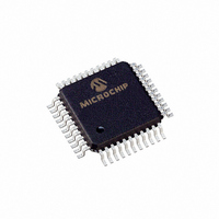
TC7129CKW Microchip Technology, TC7129CKW Datasheet - Page 5

TC7129CKW
Manufacturer Part Number
TC7129CKW
Description
IC ADC 4 1/2DGT LCD DVR 44-MQFP
Manufacturer
Microchip Technology
Datasheet
1.TC7129CPL.pdf
(28 pages)
Specifications of TC7129CKW
Display Type
LCD
Configuration
7 Segment
Digits Or Characters
A/D 4.5 Digits
Current - Supply
800µA
Voltage - Supply
6 V ~ 12 V
Operating Temperature
0°C ~ 70°C
Mounting Type
Surface Mount
Package / Case
44-MQFP, 44-PQFP
Lead Free Status / RoHS Status
Lead free / RoHS Compliant
Interface
-
Available stocks
Company
Part Number
Manufacturer
Quantity
Price
Company:
Part Number:
TC7129CKW
Manufacturer:
Microchip Technology
Quantity:
151
Company:
Part Number:
TC7129CKW
Manufacturer:
Microchip Technology
Quantity:
10 000
Company:
Part Number:
TC7129CKW713
Manufacturer:
MICROCHIP
Quantity:
12 000
Company:
Part Number:
TC7129CKW713
Manufacturer:
Microchip Technology
Quantity:
10 000
2.0
Descriptions of the pins are listed in Table 2-1.
TABLE 2-1:
© 2006 Microchip Technology Inc.
40-Pin PDIP
Pin No.
10
11
12
13
14
15
16
17
18
19
20
21
22
23
24
25
26
27
28
29
30
31
32
33
34
35
1
2
3
4
5
6
7
8
9
PIN DESCRIPTIONS
44-Pin PQFP
Pin No.
PIN FUNCTION TABLE
40
41
42
43
44
10
12
13
14
15
16
18
19
20
21
22
23
24
25
26
27
29
30
31
32
33
11
1
2
3
4
5
7
8
9
44-Pin PLCC
Pin No.
10
11
13
14
15
16
17
18
19
20
21
22
24
25
26
27
28
29
30
31
32
33
35
36
37
38
39
2
3
4
5
6
7
8
9
ANNUNCIATOR
B
B
LATCH/HOLD
CONTINUITY
3
F
F
F
B
F
1
COMMON
A
A
A
A
, C
LO BATT
, C
INT OUT
BUFFER
1
2
3
4
4
Symbol
DP
REF LO
DP
1
2
3
4
REF HI
, E
B
, E
, E
, C
, E
INT IN
C
C
OSC1
OSC3
IN LO
V
, G
, G
, G
, D
IN HI
2
3
BP
BP
BP
1
REF
REF
DISP
V–
V+
, C
, MINUS
4
3
, CONT
1
2
3
4
4
4
/OR
/UR
1
, DP
2
, DP
3
, DP
, DP
, BC
3
2
1
, G
, D
, D
, D
2
+
–
,
1
2
3
4
1
2
3
4
5
Input to first clock inverter.
Output of second clock inverter.
Backplane square wave output for driving annunciators.
Output to display segments.
Output to display segments.
Output to display segments.
Output to display segments.
Output to display segments.
Output to display segments.
Output to display segments.
Output to display segments.
Output to display segments.
Output to display segments.
Output to display segments.
Output to display segments.
Backplane #3 output to display.
Backplane #2 output to display.
Backplane #1 output to display.
Negative rail for display drivers.
Input: When high, turns on most significant decimal point.
Output: Pulled high when result count exceeds ±19,999.
Input: Second-most significant decimal point on when high.
Output: Pulled high when result count is less than ±1000.
Input: When floating, ADC operates in Free Run mode. When
pulled high, the last displayed reading is held. When pulled low,
the result counter contents are shown incrementing during the
de-integrate phase of cycle.
Output: Negative going edge occurs when the data latches are
updated. Can be used for converter status signal.
Negative power supply terminal.
Positive power supply terminal and positive rail for display
drivers.
Input to integrator amplifier.
Output of integrator amplifier.
Input: When low, continuity flag on the display is off. When high,
continuity flag is on.
Output: High when voltage between inputs is less than +200 mV.
Low when voltage between inputs is more than +200 mV.
Sets common mode voltage of 3.2V below V+ for DE, 10X, etc.
Can be used as pre-regulator for external reference.
Positive side of external reference capacitor.
Negative side of external reference capacitor.
Output of buffer amplifier.
Negative input voltage terminal.
Positive input voltage terminal.
Positive reference voltage.
Negative reference voltage
Function
TC7129
DS21459D-page 5


