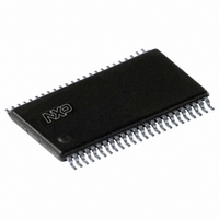
PCF8562TT/2,118 NXP Semiconductors, PCF8562TT/2,118 Datasheet - Page 15

PCF8562TT/2,118
Manufacturer Part Number
PCF8562TT/2,118
Description
IC LCD DRIVER 32/128SEG 48-TSSOP
Manufacturer
NXP Semiconductors
Datasheet
1.PCF8562TT2118.pdf
(37 pages)
Specifications of PCF8562TT/2,118
Package / Case
48-TSSOP
Display Type
LCD
Configuration
7 Segment + DP, 14 Segment (32 Segment)
Interface
I²C
Current - Supply
32µA
Voltage - Supply
1.8 V ~ 5.5 V
Operating Temperature
-40°C ~ 85°C
Mounting Type
Surface Mount
Number Of Digits
16
Number Of Segments
32
Maximum Clock Frequency
2640 Hz
Operating Supply Voltage
1.8 V to 5.5 V
Maximum Power Dissipation
400 mW
Maximum Operating Temperature
+ 85 C
Attached Touch Screen
No
Maximum Supply Current
20 uA
Minimum Operating Temperature
- 40 C
Lead Free Status / RoHS Status
Lead free / RoHS Compliant
For Use With
OM6292 - DEMO BOARD PCA2125 RTCOM10088 - KIT FOR LCD DEMO LPC900622-1003 - KIT FOR LCD DEMO
Digits Or Characters
-
Lead Free Status / Rohs Status
Lead free / RoHS Compliant
Other names
568-2029-2
PCF8562TT/2,518
PCF8562TT/2-T
PCF8562TT/2,518
PCF8562TT/2-T
NXP Semiconductors
PCF8562_5
Product data sheet
7.10 Display RAM
The display RAM is a static 32 × 4-bit RAM which stores LCD data. A logic 1 in the RAM
bit-map indicates the on-state of the corresponding LCD element; similarly, a logic 0
indicates the off-state. There is a one-to-one correspondence between the RAM
addresses and the segment outputs, and between the individual bits of a RAM word and
the backplane outputs. The display RAM bit map
correspond with the backplane outputs BP0 to BP3, and the columns 0 to 31 which
correspond with the segment outputs S0 to S31. In multiplexed LCD applications the
segment data of the first, second, third and fourth row of the display RAM are
time-multiplexed with BP0, BP1, BP2 and BP3 respectively.
When display data is transmitted to the PCF8562, the display bytes received are stored in
the display RAM in accordance with the selected LCD drive mode. The data is stored as it
arrives and does not wait for an acknowledge cycle as with the commands. Depending on
the current multiplex drive mode, data is stored singularly, in pairs, triplets or quadruplets.
To illustrate the filling order, an example of a 7-segment numeric display showing all drive
modes is given in
LCD types.
The following applies to
Fig 9.
•
•
•
•
In the static drive mode, the eight transmitted data bits are placed in row 0 of eight
successive 4-bit RAM words.
In the 1:2 multiplex mode, the eight transmitted data bits are placed in pairs into
row 0 and 1 of four successive 4-bit RAM words.
In the 1:3 multiplex mode, the eight bits are placed in triples into row 0, 1 and 2 to
three successive 4-bit RAM words, with bit 3 of the third address left unchanged. It is
not recommended to use this bit in a display because of the difficult addressing. This
last bit may, if necessary, be controlled by an additional transfer to this address but
care should be taken to avoid overwriting adjacent data because always full bytes are
transmitted.
In the 1:4 multiplex mode, the eight transmitted data bits are placed in quadruples into
row 0, 1, 2 and 3 of two successive 4-bit RAM words.
display RAM rows/
backplane outputs
Display RAM bit map showing direct relationship between RAM addresses and segment outputs;
also between bits in a RAM word and the backplane outputs.
Display RAM bit map
rows
(BP)
All information provided in this document is subject to legal disclaimers.
Figure
0
1
2
3
Rev. 05 — 19 May 2010
Figure
0
10; the RAM filling organization depicted applies equally to other
1
10:
2
3
display RAM addresses/segment outputs (S)
4
Universal LCD driver for low multiplex rates
Figure 9
columns
shows the rows 0 to 3 which
27
28
PCF8562
© NXP B.V. 2010. All rights reserved.
29
001aac265
30
31
15 of 37


