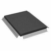
AD9884AKSZ-140 Analog Devices Inc, AD9884AKSZ-140 Datasheet

AD9884AKSZ-140
Specifications of AD9884AKSZ-140
Available stocks
Related parts for AD9884AKSZ-140
AD9884AKSZ-140 Summary of contents
Page 1
FEATURES 140 MSPS Maximum Conversion Rate 500 MHz Analog Bandwidth 0 1.0 V Analog Input Range 400 ps p-p PLL Clock Jitter Power-Down Mode 3.3 V Power Supply 2 3.3 V Three-State CMOS Outputs Demultiplexed ...
Page 2
AD9884A–SPECIFICATIONS Parameter Temp RESOLUTION DC ACCURACY Differential Nonlinearity 25°C Full Integral Nonlinearity 25°C Full No Missing Codes Full ANALOG INPUT Input Voltage Range Minimum Full Maximum Full Gain Tempco 25°C Input Bias Current 25°C Full Input Offset Voltage Full Input ...
Page 3
Parameter POWER SUPPLY V Supply Voltage D V Supply Voltage DD PV Supply Voltage D I Supply Current ( Supply Current ( IPV Supply Current ( Total Power Dissipation ...
Page 4
AD9884A Signal Type Name Function Inputs R Analog Input for RED Channel AIN G Analog Input for GREEN Channel AIN B Analog Input for BLUE Channel AIN HSYNC Horizontal Sync Input COAST Clock Generator Coast Input (Optional) 3.3 V CMOS ...
Page 5
GND 6 GND R 7 AIN GND GND 13 GND 14 SOGIN 15 G AIN GND ...
Page 6
AD9884A Pin Name Function INPUTS R Analog Input for RED Channel AIN G Analog Input for GREEN Channel AIN B Analog Input for BLUE Channel AIN High impedance inputs that accepts the RED, GREEN, and BLUE channel graphics signals, respectively. ...
Page 7
Pin Name Function OUTPUTS D A Data Output, Red Channel, Port A R 7– Data Output, Red Channel, Port B R 7– Data Output, Green Channel, Port A G 7– Data Output, Green Channel, ...
Page 8
AD9884A Pin Name Function ANALOG INTERFACE REFOUT Internal Reference Output Output from the internal 1.25 V bandgap reference. This output is intended to drive relatively light loads. It can drive the AD9884A Reference input directly, but should be externally buffered ...
Page 9
CONTROL REGISTER MAP The AD9884A is initialized and controlled by a set of registers that determine the operating modes. An external controller is employed to write and read the control registers through the 2-line serial interface port. Table II. Control ...
Page 10
AD9884A INPUT GAIN 02 7–0 REDGAIN Red Channel Gain Adjust An 8-bit word that sets the gain of the RED channel. The AD9884A can accommodate input signals with a full-scale range of between 0.5 V and 1.0 V p-p. Setting ...
Page 11
GENERAL CONTROL 0A 7 DEMUX Output Port Select A bit that determines whether all pixels are presented to a single port (A), or alternating pixels are demultiplexed to Ports A and B. DEMUX Function 0 All Data Goes to Port ...
Page 12
AD9884A CLOCK GENERATOR CONTROL 0B 7–3 PHASE Clock Phase Adjust A five-bit value that adjusts the sampling phase in 32 steps across one pixel time. Each step represents an 11.25 degree shift in sampling phase. The power-up default value is ...
Page 13
Writing data to specific control registers of the AD9884A requires that the 8-bit address of the control register of interest be written after the slave address has been established. This control register address is the base address for subsequent write ...
Page 14
AD9884A 800 700 600 500 400 100 FREQUENCY – Mpps Figure 3. Power Dissipation vs. Frequency DESIGN GUIDE GENERAL DESCRIPTION The AD9884A is a fully-integrated solution for capturing analog RGB signals and digitizing them for ...
Page 15
In typical PC-based graphic systems, the sync signals are simply TTL-level drivers feeding unshielded wires in the monitor cable. Since the AD9884A operates from a 3.3 V power supply, and TTL sources may drive a high level ...
Page 16
AD9884A OFFSET = 3FH OFFSET = 1FH 1.0V OFFSET = 0FH 0.5V OFFSET = 3FH OFFSET = 1FH OFFSET = 0FH 0.0V 00h GAIN Figure 8. Gain and Offset Control CLOCK GENERATION A Phase Locked Loop (PLL) is employed to ...
Page 17
Table VII. Recommended VCORNGE and CURRENT Settings for Standard Display Formats Standard Resolution 640 × 480 VGA 800 × 600 SVGA 1024 × 768 XGA 1280 × 1024 SXGA 1600 × 1200 UXGA VESA Monitor Timing Standards and Guidelines, September ...
Page 18
AD9884A TIMING The following timing diagrams show the operation of the AD9884A in all clock modes. The part establishes timing by having the sample that corresponds to the pixel digitized when the leading edge of HSYNC occurs sent to the ...
Page 19
ALTERNATE PIXEL SAMPLING MODE A Logic 1 input on CKINV (Pin 27) shifts the sampling phase 180 degrees. CKINV can be switched between frames to imple- ment the alternate pixel sampling mode. This allows higher effective image resolution to be ...
Page 20
AD9884A RGBIN P0 P1 HSYNC PXCK HS 5 PIPE DELAY ADCCK DATACK DOUTA HSOUT RGBIN HSYNC PXCK HS 5 PIPE DELAY ADCCK DATACK DOUTA HSOUT Figure 19. Single Channel Mode, Alternate Pixel Sampling (Even ...
Page 21
P0 P1 RGBIN HSYNC PXCK HS ADCCK DATACK DOUTA HSOUT RGBIN HSYNC PXCK HS 5 PIPE DELAY ADCCK DATACK DOUTA DOUTB HSOUT Figure 23. Dual Channel Mode, Interleaved Outputs, Alternate Pixel Sampling (Even Pixels) ...
Page 22
AD9884A RGBIN HSYNC PXCK HS ADCCK DATACK DOUTA DOUTB HSOUT Figure 26. Dual Channel Mode, Parallel Outputs, Alternate Pixel Sampling (Odd Pixels) PCB LAYOUT RECOMMENDATIONS The AD9884A is a high precision, high speed analog ...
Page 23
In some cases, using separate ground planes is unavoidable. For those cases, we recommend to at least place a single ground plane under the AD9884A. The location of the split should be at the receiver of the digital outputs. For ...
Page 24
AD9884A 0.041 (1.03) 0.035 (0.88) 0.031 (0.78) SEATING PLANE 0.003 (0.08) MAX 0.010 (0.25) MIN Revision History Location Data Sheet changed from REV REV. C. Edit to ABSOLUTE MAXIMUM RATINGS . . . . . . . . ...


