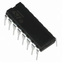
HCF4511BEY STMicroelectronics, HCF4511BEY Datasheet

HCF4511BEY
Specifications of HCF4511BEY
Related parts for HCF4511BEY
HCF4511BEY Summary of contents
Page 1
... Lamp Test (LT), Blanking (BL), and Latch Enable Semiconductor or Strobe inputs are provided to test the display, shut off or intensity-modulate it, and store or strobe a BCD code, respectively. Several different signals may be multiplexed and displayed when external multiplexing circuitry is used. HCF4511B DIP SOP TUBE T & R HCF4511BEY HCF4511BM1 HCF4511M013TR 1/13 ...
Page 2
HCF4511B INPUT EQUIVALENT CIRCUIT FUNCTIONAL DIAGRAM 2/13 PIN DESCRIPTION PIN No SYMBOL NAME AND FUNCTION Bcd Inputs 13, 12, 11 7-Segment Outputs 10 Lamp ...
Page 3
LOGIC DIAGRAM TRUTH TABLE ...
Page 4
HCF4511B ABSOLUTE MAXIMUM RATINGS Symbol V Supply Voltage Input Voltage Input Current I P Power Dissipation per Package D Power Dissipation per Output Transistor T Operating Temperature op T Storage Temperature stg Absolute Maximum ...
Page 5
DC SPECIFICATIONS Symbol Parameter V (V) I Quiescent Current 0/5 L 0/10 0/15 0/20 V High Level Output 0/5 OH Voltage 0/10 0/15 V Low Level Output 5/0 OL Voltage 10/0 15/0 V High Level Input IH Voltage V Low ...
Page 6
HCF4511B DYNAMIC ELECTRICAL CHARACTERISTICS (T Symbol Parameter t Propagation Delay Time PHL (DATA) t Propagation Delay Time PLH (DATA) t Propagation Delay Time PHL (BL) t Propagation Delay Time PLH (BL) t Propagation Delay Time PHL (LT) t Propagation Delay ...
Page 7
TYPICAL APPLICATIONS (Interfacing with various displays) Driving Common-cathode 7 Segment Led Displays Driving Low-voltage Fluorescent Displays A medium-brightness intensity display can be obtained with low-voltage fluorescent displays such as the Tung-Sot Digi- vac S/G series Driving Incandescent Displays 2 Of ...
Page 8
HCF4511B TEST CIRCUIT C = 50pF or equivalent (includes jig and probe capacitance 200K pulse generator (typically OUT WAVEFORM 1 : PROPAGATION DELAY TIMES (f=1MHz; 50% duty cycle) 8/13 ...
Page 9
WAVEFORM 2 : MINIMUM PULSE WIDTH (f=1MHz; 50% duty cycle) WAVEFORM 3 : PROPAGATION DELAY TIMES (f=1MHz; 50% duty cycle) HCF4511B 9/13 ...
Page 10
HCF4511B WAVEFORM 4 : PROPAGATION DELAY TIMES (f=1MHz; 50% duty cycle) WAVEFORM 5 : MINIMUM SETUP AND HOLD TIME (f=1MHz; 50% duty cycle) 10/13 ...
Page 11
Plastic DIP-16 (0.25) MECHANICAL DATA mm. DIM. MIN. TYP a1 0.51 B 0.77 b 0 8.5 e 2.54 e3 17. 3.3 Z inch MAX. MIN. TYP. 0.020 1.65 0.030 0.020 0.010 20 0.335 ...
Page 12
HCF4511B DIM. MIN 0 0. 9 3.8 G 4 12/13 SO-16 MECHANICAL DATA mm. TYP MAX. 1.75 0.2 1.65 0.46 0.25 0.5 ...
Page 13
... No license is granted by implication or otherwise under any patent or patent rights of STMicroelectronics. Specifications its use. No license is granted by implication or otherwise under any patent or patent rights of STMicroelectronics. Specifications mentioned in this publication are subject to change without notice. This publication supersedes and replaces all information mentioned in this publication are subject to change without notice ...


