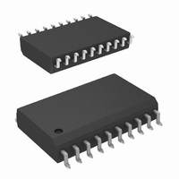
COP472WM-3/NOPB National Semiconductor, COP472WM-3/NOPB Datasheet - Page 6

COP472WM-3/NOPB
Manufacturer Part Number
COP472WM-3/NOPB
Description
IC LCD DISPLAY DRIVER 20-SOIC
Manufacturer
National Semiconductor
Datasheet
1.COP472WM-3NOPB.pdf
(8 pages)
Specifications of COP472WM-3/NOPB
Display Type
LCD
Configuration
36 Segment
Interface
Serial
Digits Or Characters
4.5 Digits
Current - Supply
250µA
Voltage - Supply
3 V ~ 5.5 V
Operating Temperature
0°C ~ 70°C
Mounting Type
Surface Mount
Package / Case
20-SOIC (7.5mm Width)
Operating Supply Voltage (typ)
3.3/5V
Number Of Digits
4.5
Number Of Segments
36
Operating Temperature (min)
0C
Operating Temperature (max)
70C
Operating Temperature Classification
Commercial
Package Type
SOIC W
Pin Count
20
Mounting
Surface Mount
Frequency (max)
250KHz
Operating Supply Voltage (min)
3V
Operating Supply Voltage (max)
5.5V
No. Of Digits / Alpha
4-1/2
No. Of Segments
36
Meter Display Type
LCD
Interface Type
Triplexed
Supply Voltage Range
3V To 5.5V
Driver Case Style
SOIC
No. Of Pins
20
Rohs Compliant
Yes
Lead Free Status / RoHS Status
Lead free / RoHS Compliant
Other names
COP472WM-3
Available stocks
Company
Part Number
Manufacturer
Quantity
Price
Company:
Part Number:
COP472WM-3/NOPB
Manufacturer:
NS
Quantity:
10 359
http
LOADING SEQUENCE TO DRIVE A 4 -DIGIT DISPLAY
Steps
1
2
3
4
5
6
7
Note CS may be turned high after any step For example to
load only 2 digits of data do steps 1 2 3 and 7
CS must make a high to low transition before loading data in
order to reset internal counters
LOADING SEQUENCE TO DRIVE AN
8 -DIGIT DISPLAY
Two or more COP472-3’s may be connected together to
drive additional segments An eight digit multiplexed display
is shown in Figure 7 The following is the loading sequence
to drive an eight digit display using two COP472-3’s The
right chip is the master and the left the slave
Steps
1
2
3
4
5
6
7
8
The chips are now synchronized and driving 8 digits of dis-
play To load new data simply load each chip separately in
the normal manner keeping the correct status bits to each
COP472-3 (0110 or 0001)
www national com
0
1
0
Turn CE low
Clock in 8 bits of data for digit 1
Clock in 8 bits of data for digit 2
Clock in 8 bits of data for digit 3
Clock in 8 bits of data for digit 4
Clock in 8 bits of data for special segment and control
function of BPC and BPA
Turn CS high
Turn CS low on both COP472-3’s
Shift in 32 bits of data for the slave’s four digits
Shift in 4 bits of special segment data a zero and three
ones
This synchronizes both the chips and BPA is oscillator
input Both chips are now stopped
Turn CS high to both chips
Turn CS low to master COP472-3
Shift in 32 bits of data for the master’s 4 digits
Shift in four bits of special segment data a one and
three zeros
This sets the master COP472-3 to BPA as a normal
backplane output and BPC as oscillator output Now
both the chips start and run off the same oscillator
Turn CS high
0
1
0
1
1
0
1
0
1
SP4
SP4
SP4
SP3
SP3
SP3
SP2
SP2
SP2
SP1
SP1
SP1
6
FIGURE 6 System Diagram – 4
FIGURE 7 System Diagram – 8
Digit Display
Digit Display
TL DD 6932 – 6
TL DD 6932 – 7


