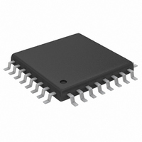
MAX1494CCJ+T Maxim Integrated Products, MAX1494CCJ+T Datasheet - Page 23

MAX1494CCJ+T
Manufacturer Part Number
MAX1494CCJ+T
Description
IC ADC W/LCD DRIVER 32-TQFP
Manufacturer
Maxim Integrated Products
Datasheet
1.MAX1494CCJ.pdf
(34 pages)
Specifications of MAX1494CCJ+T
Display Type
LCD
Configuration
7 Segment + 2 Annunciators
Interface
Serial
Digits Or Characters
A/D 4.5 Digits
Current - Supply
960µA
Voltage - Supply
2.7 V ~ 5.25 V
Operating Temperature
0°C ~ 70°C
Mounting Type
Surface Mount
Package / Case
32-LQFP
Lead Free Status / RoHS Status
Lead free / RoHS Compliant
SPI/ADC:
EXTCLK:
INTREF:
DP_EN:
DPSET[2:1]:
HOLD:
PEAK:
PD_ANA:
PD_DIG:
(Default = 0) Display Select Bit. The
SPI/ADC bit controls selection of the
data fed into the LCD data register. A
1 in this location selects SPI/QSPI/
MICROWIRE data (the user writes this
data to the LCD data register). A 0 in
this location selects the ADC result
register data, unless hold or peak
functions are active (Table 6).
(Default = 0) External Clock Select
Bit. The EXTCLK bit controls selec-
tion of the internal clock or an exter-
nal clock source. A 1 in this location
selects the signal at the CLK input as
the clock source. A 0 in this location
selects the internal clock oscillator.
Toggle the PD_DIG and PD_ANA
after changing the EXTCLK bit.
(Default = 0) Reference Select Bit. For
internal reference operation, set
INTREF to 1. For external reference
operation, set INTREF to 0.
(Default = 0) Decimal-Point Enable
Bit (Tables 2 and 3).
(Default
Selection Bits (Tables 2 and 3).
(Default = 0) Hold Bit. When set to 1,
the LCD register does not update
from the ADC conversion results and
holds the last result on the LCD. The
MAX1492/MAX1494 continue to per-
form conversions during HOLD
(Table 6).
(Default = 0) Peak Bit. When set to 1
(and the HOLD bit is set to 0), the
LCD shows the result stored in the
peak register (Table 6).
(Default = 0) Power-Down Analog
Select Bit. When set to 1, the analog
circuits (analog modulator and ADC
input buffers) go into the power-down
mode. When set to 0, the device is in
full power-up mode.
(Default = 0) Power-Down Digital
Select Bit. When set to 1, the digital
circuits (digital filter and LCD drivers)
go into power-down mode. This also
resets the values of the internal
SRAM (in the digital filter) to zeros.
When set to 0, the device returns to
full power-up mode.
______________________________________________________________________________________
=
3.5- and 4.5-Digit, Single-Chip ADCs
00)
Decimal-Point
RANGE:
CLR:
SEG_SEL:
OFFSET_CAL1: (Default = 0) Automatic-Offset Enable
OFFSET_CAL2: (Default = 0) Enhanced Offset-
Note: When changing any one of the following control
bits: OFFSET_CAL1, RANGE, PD_ANA, PD_DIG,
INTREF, and EXTCLK, wait 800ms before reading the
ADC results.
with LCD Drivers
(Default = 0) Input-Range Select Bit.
When set to 0, the input voltage
range is ±2V. When set to 1, the input
voltage range is ±200mV. Toggle the
PD_DIG and PD_ANA after changing
the RANGE bit.
(Default = 0) Clear-All-Registers Bit.
When set to 1, all the registers reset
to their power-on reset states when
CS makes a low-to-high transition.
(Default = 0) LCD Segment-Selection
Bit. When set to 1, the LCD segment
drivers use the LCD segment regis-
ters to display individual segments
that can form letters or numbers or
other information on the display. The
LCD data register is NOT displayed.
Send the data first to the LCD seg-
ment-display registers and then set
this bit high (Table 6).
Bit. When set to 1, the MAX1492/
MAX1494 disable automatic offset cali-
bration. When this bit is set to 0, auto-
matic offset calibration is enabled.
Calibration Start Bit (MAX1494 Only
and RANGE = 1). To achieve the low-
est possible offset in the ±200mV
input range, perform an enhanced
offset calibration by setting this bit to
1. The calibration takes approximate-
ly 9 cycles (1800ms). After the cali-
bration completes, set this bit to 0 to
resume ADC conversions.
23


