MM74C911N Fairchild Semiconductor, MM74C911N Datasheet
MM74C911N
Specifications of MM74C911N
74C911N
Available stocks


Related parts for MM74C911N


MM74C911N Summary of contents
Page 1
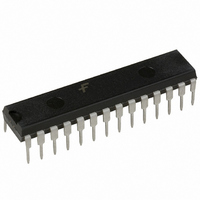
... N28B 28-Lead Plastic Dual-In-Line Package (PDIP), JEDEC MS 010, 0.600” Wide Connection Diagram © 1999 Fairchild Semiconductor Corporation The digit outputs directly drive the base of the digit transis- tor when the control pin labeled DIGIT INPUT OUTPUT, DIO, is LOW. When DIO is HIGH, the digit lines turn into inputs and the internal scanning multiplexer is disabled ...
Page 2
Truth Tables Input Control Digit CE Address Write Digit Latch Digit Write Digit Latch Digit ...
Page 3
Absolute Maximum Ratings (Note 2) Voltage at Any Pin except Inputs 0. Voltage at Any Input except Digits Operating Temperature Range Storage Temperature Range Power Dissipation (P ) Refer D(MAX) DC Electrical ...
Page 4
AC Electrical Characteristics Symbol Parameter t Chip Enable to Write Enable Set-Up Time CW t Address to Write Enable Set-Up Time AW t Write Enable Width WW ...
Page 5
Switching Time Waveforms Multiplexing Output Waveforms Typical Performance Characteristics Segment outputs if shorted to ground will exceed maximum power dissipation of the device. Applications Segment Output Structure (Continued) Read Data Waveforms Note A: All other digit lines are at a ...
Page 6
Input Protection Segment Expansion Typical Application 6 ...
Page 7
Alpha-Numeric Display Segment Identification 7 www.fairchildsemi.com ...
Page 8
Physical Dimensions inches (millimeters) unless otherwise noted 28-Lead Plastic Dual-In-Line Package (PDIP), JEDEC MS-010, 0.600” Wide LIFE SUPPORT POLICY FAIRCHILD’S PRODUCTS ARE NOT AUTHORIZED FOR USE AS CRITICAL COMPONENTS IN LIFE SUPPORT DEVICES OR SYSTEMS WITHOUT THE EXPRESS WRITTEN APPROVAL ...