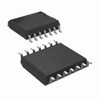
LM5067MW-1/NOPB National Semiconductor, LM5067MW-1/NOPB Datasheet

LM5067MW-1/NOPB
Specifications of LM5067MW-1/NOPB
Available stocks
Related parts for LM5067MW-1/NOPB
LM5067MW-1/NOPB Summary of contents
Page 1
... In-rush current limit for safe board insertion into live power sources ■ Programmable maximum power dissipation in the external pass device Typical Application © 2009 National Semiconductor Corporation LM5067 ■ Adjustable current limit ■ Circuit breaker function for severe over-current events ■ ...
Page 2
... Connection Diagrams Top View 10-Lead MSOP Ordering Information Order Number Fault Response LM5067MM-1 Latch Off LM5067MMX-1 Latch Off LM5067MM-2 Auto Restart LM5067MMX-2 Auto Restart LM5067MW-1 Latch Off LM5067MWX-1 Latch Off Pin Descriptions Pin # Name MSOP-10 SO- VCC 2 3 UVLO/ OVLO 4 5 PWR ...
Page 3
Pin # Name Description MSOP-10 SO- OUT Output feedback Connect to the external MOSFET’s drain. Internally used to determine the 10 14 PGD Power Good indicator Applications Information MOSFET V voltage for power limiting, and to control the ...
Page 4
... Absolute Maximum Ratings If Military/Aerospace specified devices are required, please contact the National Semiconductor Sales Office/ Distributors for availability and specifications. Current into VCC (100 µs pulse) OUT, PGD to VEE UVLO, OVLO to VEE SENSE to VEE ESD Rating (Note 2) Human Body Model Electrical Characteristics junction temperature (T ) range of -40° ...
Page 5
... Note 3: Current out of a pin is indicated as a negative value. Note 4: For detailed information on soldering plastic MSOP package refer to the Packaging Databook available from National Semiconductor Corporation. Note 5: Maximum continuous current into VCC is limited by power dissipation and die temperature. See the Thermal Considerations section. ...
Page 6
Typical Performance Characteristics apply 25° vs. Operating Voltage - Disabled CC Operating Voltage vs. I OUT Pin Current vs. System Voltage www.national.com Unless otherwise specified the following conditions I vs. Operating Voltage - Enabled CC 30030904 ...
Page 7
GATE Pull-Down Current, Circuit Breaker vs. GATE Voltage MOSFET Power Dissipation Limit vs. R UVLO, OVLO Threshold Voltage vs. Temperature PGD Low Voltage vs. Sink Current 30030910 and R UVLO & OVLO Hysteresis Current vs. Temperature PWR S 30030912 V ...
Page 8
Current Limit Threshold vs. Temperature Power Limit Threshold vs. Temperature GATE Pull-Down Current, Circuit Breaker vs. Temperature www.national.com Circuit Breaker Threshold vs. Temperature 30030917 Gate Source Current vs. Temperature 30030919 PGD Pin Low Voltage vs. Temperature 30030921 8 30030918 30030920 ...
Page 9
POR Threshold vs. Temperature EN TIMER Pin Fault Detection Current vs. Temperature TIMER Pin Thresholds vs. Temperature 30030923 30030926 9 30030925 www.national.com ...
Page 10
Block Diagram www.national.com FIGURE 1. Basic Application Circuit 10 30030927 30030928 ...
Page 11
Functional Description The LM5067 is designed to control the in-rush current to the load upon insertion of a circuit card into a live backplane or other “hot” power source, thereby limiting the voltage sag on the backplane’s supply voltage, and ...
Page 12
Operating Voltage The LM5067 operating voltage is the voltage from VCC to VEE. The maximum operating voltage is set by an internal 13V zener diode. With the IC connected as shown in Figure 1, the LM5067 controller operates in the ...
Page 13
If the system input voltage falls below the UVLO threshold, or rises above the OVLO threshold, the GATE pin is pulled low by the 2.2 mA pull-down current to switch off Q1. FIGURE 4. Gate Control Current Limit The current ...
Page 14
Under-Voltage Lock-Out (UVLO) The series pass MOSFET (Q1) is enabled when the input supply voltage ( within the operating range defined by SYS the programmable under-voltage lockout (UVLO) and over- voltage lock-out (OVLO) levels. Typically the UVLO level ...
Page 15
SENSE to VEE. The required resistor S value is calculated from: where I is the desired current limit threshold. When the LIM voltage across R reaches 50 mV, the current limit circuit S modulates the gate ...
Page 16
FIGURE 9. Load Draws Current During Turn-On B) Turn-on with power limit and current limit: The power dissipation limit defined by the resistor at FET(LIM) the PWR pin, and the current sense resistor R www.national.com ...
Page 17
MOSFET SELECTION It is recommended that the external MOSFET (Q1) selection be based on the following criteria: - The BV rating should be greater than the maximum DSS system voltage (V ), plus ringing and transients which can SYS occur ...
Page 18
The procedure to calculate the resistor values is as follows: - Determine the upper UVLO threshold (V Q1, and the lower UVLO threshold (V - Determine the upper OVLO threshold (V Q1. - The lower OVLO threshold (V OVL be ...
Page 19
As an example, assume the application requires the following thresholds -22V -17V, V UVH UVL V = -58V. Therefore V = 5V, and V OVL UV(HYS) resistor values are 227 kΩ 39.1 ...
Page 20
POWER GOOD PIN During initial power up, the Power Good pin (PGD) is high until the operating voltage (VCC – VEE) increases above PGD then switches low, remaining low as the system voltage and the operating voltage increase. After Q1 ...
Page 21
PC Board Guidelines The following guidelines should be followed when designing the PC board for the LM5067: • Place the LM5067 close to the board’s input connector to minimize trace inductance from the connector to the FET. • Place R ...
Page 22
Thermal Considerations The LM5067 should be operated so that its junction temper- ature does not exceed 125°C. The junction temperature is equal to θ where T is the ambient temperature, and R A ...
Page 23
Physical Dimensions inches (millimeters) unless otherwise noted NS Package Number MUB10A NS Package Number M14B 23 www.national.com ...
Page 24
... For more National Semiconductor product information and proven design tools, visit the following Web sites at: Products Amplifiers www.national.com/amplifiers Audio www.national.com/audio Clock and Timing www.national.com/timing Data Converters www.national.com/adc Interface www.national.com/interface LVDS www.national.com/lvds Power Management www.national.com/power Switching Regulators www.national.com/switchers LDOs www.national.com/ldo LED Lighting www ...


