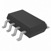
LTC4361CTS8-1#TRPBF Linear Technology, LTC4361CTS8-1#TRPBF Datasheet

LTC4361CTS8-1#TRPBF
Specifications of LTC4361CTS8-1#TRPBF
Available stocks
Related parts for LTC4361CTS8-1#TRPBF
LTC4361CTS8-1#TRPBF Summary of contents
Page 1
... After an overcurrent fault, the LTC4361-1 remains off while the LTC4361-2 automatically restarts after a 130ms start-up delay. L, LT, LTC, LTM, Linear Technology and the Linear logo are registered trademarks and ThinSOT, Hot Swap SENSE Corporation. All other trademarks are the property of their respective owners. ...
Page 2
... GATEP 3 GND 4 TS8 PACKAGE 8-LEAD PLASTIC TSOT-23 = 125°C, θ 195°C/W JMAX JA ORDER INFORMATION Lead Free Finish TAPE AND REEL (MINI) TAPE AND REEL LTC4361CTS8-1#TRMPBF LTC4361CTS8-1#TRPBF LTC4361CTS8-2#TRMPBF LTC4361CTS8-2#TRPBF LTC4361ITS8-1#TRMPBF LTC4361ITS8-1#TRPBF LTC4361ITS8-2#TRMPBF LTC4361ITS8-2#TRPBF LTC4361CDC-1#TRMPBF LTC4361CDC-1#TRPBF LTC4361CDC-2#TRMPBF LTC4361CDC-2#TRPBF LTC4361IDC-1#TRMPBF LTC4361IDC-1#TRPBF LTC4361IDC-2#TRMPBF LTC4361IDC-2#TRPBF TRM = 500 pieces. *Temperature grades are identifi ...
Page 3
ELECTRICAL CHARACTERISTICS temperature range, otherwise specifi cations are at T SYMBOL PARAMETER Supplies V Input Voltage Range IN V Input Undervoltage Lockout IN(UVL) I Input Supply Current IN Thresholds V IN Pin Overvoltage Threshold IN(OV) ∆V Overvoltage Hysteresis OV ∆V ...
Page 4
LTC4361-1/LTC4361-2 TYPICAL PERFORMANCE CHARACTERISTICS T = 25° 5V 0V, unless otherwise noted Input Supply Current vs Input Voltage 10000 1000 100 0.1 1 ...
Page 5
PIN FUNCTIONS Exposed Pad (DFN): Ground. Connection to PCB is optional. GATE: Gate Drive for External N-Channel MOSFET. An internal charge pump provides a 10μA pull-up current to charge the gate of the external N-channel MOSFET. An additional ramp circuit ...
Page 6
LTC4361-1/LTC4361-2 OPERATION Mobile devices like cell phones and MP3/MP4 players have highly integrated subsystems fabricated from deep submi- cron CMOS processes. The small form factor is accompanied by low absolute maximum voltage ratings. The sensitive electronics are susceptible to damage ...
Page 7
APPLICATIONS INFORMATION The typical LTC4361 application protects 2.5V to 5.5V systems in portable devices from power supply overvolt- age. The basic application circuit is shown in Figure 1. Device operation and external component selection is discussed in detail in the ...
Page 8
LTC4361-1/LTC4361-2 APPLICATIONS INFORMATION The LTC4361-1 has an internal latch that maintains this off state until it is reset. To reset this latch, cycle IN be above 1.5V (V low 2.1V (V IN(UVL) than 500μs. After reset, the ...
Page 9
APPLICATIONS INFORMATION ON Input CMOS compatible, active low enable input. It has a default 5μA pull-down to ground. Connect this pin to ground or leave open to enable normal device operation driven high while ...
Page 10
LTC4361-1/LTC4361-2 APPLICATIONS INFORMATION WALL ADAPTOR AC/ CABLE + CABLE WALL ADAPTOR AC/ SENSE IN I CABLE + CABLE Input Transients Figure 4 shows a typical setup when an AC ...
Page 11
APPLICATIONS INFORMATION As the IN pin can withstand up to 80V, a high voltage N- channel MOSFET can be used to protect the system against rugged abuse from high transient or DC voltages up to the BV of the MOSFET. ...
Page 12
LTC4361-1/LTC4361-2 APPLICATIONS INFORMATION Figure 8 shows a particularly severe situation which can occur in a mobile device with dual power inputs. A 20V wall adaptor is mistakenly hot-plugged into the 5V device with the USB input already live. As shown ...
Page 13
PACKAGE DESCRIPTION 2.55 ±0.05 0.64 ±0.05 1.15 ±0.05 (2 SIDES) RECOMMENDED SOLDER PAD PITCH AND DIMENSIONS APPLY SOLDER MASK TO AREAS THAT ARE NOT SOLDERED PIN 1 BAR TOP MARK (SEE NOTE 6) 0.200 REF LTC4361-1/LTC4361-2 DC Package 8-Lead Plastic ...
Page 14
LTC4361-1/LTC4361-2 PACKAGE DESCRIPTION 0.40 MAX 3.85 MAX 2.62 REF RECOMMENDED SOLDER PAD LAYOUT PER IPC CALCULATOR 0.20 BSC DATUM ‘A’ 0.30 – 0.50 REF NOTE: 1. DIMENSIONS ARE IN MILLIMETERS 2. DRAWING NOT TO SCALE 3. DIMENSIONS ARE INCLUSIVE OF ...
Page 15
... Revised GATE Control in Applications Information Section Information furnished by Linear Technology Corporation is believed to be accurate and reliable. However, no responsibility is assumed for its use. Linear Technology Corporation makes no representa- tion that the interconnection of its circuits as described herein will not infringe on existing patent rights. ...
Page 16
... M3 C OUT 10μF GATE SENSE OUT V IO LTC4361 GATEP D1 ON PWRGD LN1351CTR GND 436112 TA03 : 3μ 2.0V to 45V 0.6V to 39.5V OUT : 3μ 1.6V to 20V 0.6V to 19.5V OUT LT 0111 REV A • PRINTED IN USA © LINEAR TECHNOLOGY CORPORA TION 2010 V OUT 5V 0.5A 436112fa ...


