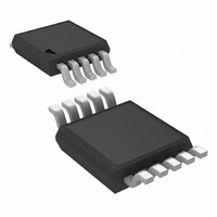
LM25061PMM-2/NOPB National Semiconductor, LM25061PMM-2/NOPB Datasheet

LM25061PMM-2/NOPB
Specifications of LM25061PMM-2/NOPB
Available stocks
Related parts for LM25061PMM-2/NOPB
LM25061PMM-2/NOPB Summary of contents
Page 1
... The LM25061-1 latches off after a fault detection, while the LM25061-2 automatically restarts at a fixed duty cycle. The LM25061 is available pin MSOP package. Typical Application © 2010 National Semiconductor Corporation LM25061 Features ■ Operating range: +2.9V to +17V ■ ...
Page 2
... Connection Diagram Ordering Information Order Number Fault Response LM25061PMME-1 Latch Off LM25061PMM-1 Latch Off LM25061PMMX-1 Latch Off LM25061PMME-2 Auto Restart LM25061PMM-2 Auto Restart LM25061PMMX-2 Auto Restart Pin Descriptions Pin # Name Description 1 SENSE Current sense input 2 VIN Positive supply input 3 UVLO/EN Under-voltage lockout ...
Page 3
... Absolute Maximum Ratings If Military/Aerospace specified devices are required, please contact the National Semiconductor Sales Office/ Distributors for availability and specifications. VIN to GND (Note 5) SENSE, OUT, PGD to GND UVLO to GND FB to GND VIN to SENSE ESD Rating (Note 2) Human Body Model Storage Temperature ...
Page 4
... Note 3: OUT bias current (disabled) due to leakage current through an internal 1.0 MΩ resistance from SENSE to VOUT. Note 4: For detailed information on soldering plastic MSOP packages refer to the Packaging Databook available from National Semiconductor Corporation. Note 5: Current out of a pin is indicated as a negative number. ...
Page 5
Typical Performance Characteristics T = 25° 12V J IN VIN Pin Input Current vs. VIN OUT Pin Input Current GATE Pin Source Current Unless otherwise specified the following conditions apply: SENSE Pin Input Current 30090303 GATE Pin Voltage ...
Page 6
PGD Pin Low Voltage vs. Sink Current UVLO Threshold vs. Temperature FB Threshold vs. Temperature www.national.com Input Current, Enabled vs. Temperature 30090308 UVLO Hysteresis Current vs. Temperature 30090357 FB Hysteresis Current vs. Temperature 30090368 6 30090358 30090355 30090369 ...
Page 7
Current Limit Threshold vs. Temperature Power Limit Threshold vs. Temperature GATE Source Current vs. Temperature Circuit Breaker Threshold vs. Temperature 30090359 GATE Output Voltage vs. Temperature 30090361 PGD Low Voltage vs. Temperature 30090363 7 30090360 30090362 30090365 www.national.com ...
Page 8
Block Diagram www.national.com 8 30090310 ...
Page 9
Functional Description The LM25061 is designed to control the in-rush current to the load upon insertion of a circuit card into a live backplane or other "hot" power source, thereby limiting the voltage sag on the backplane’s supply voltage, and ...
Page 10
During the in-rush limiting interval (t2 in Figure 3) an internal 80 µA fault timer current source charges Q1’s power dissipation and the T input current reduce below their respective ...
Page 11
If the system input voltage falls below the UVLO threshold, the GATE pin is pulled low by the 2 mA pull-down current to switch off Q1. Current Limit The current limit threshold is reached when the voltage across the sense ...
Page 12
Under-Voltage Lock-Out (UVLO) The series pass MOSFET (Q1) is enabled when the input supply voltage ( greater than the programmable un- SYS der-voltage lockout (UVLO) level. Typically the UVLO level set with a resistor divider ...
Page 13
The resistor’s surge capability must also be considered since the circuit breaker threshold is ap- proximately twice ...
Page 14
R is the load resistance. The Fault Timeout Period L must be set longer than t to prevent a fault shutdown before ...
Page 15
MOSFET SELECTION It is recommended that the external MOSFET (Q1) selection be based on the following criteria: - The BV rating should be greater than the maximum DSS system voltage (V ), plus ringing and transients which can SYS occur ...
Page 16
FIGURE 11. Programming the UVLO Thresholds The two resistor values are calculated as follows: - Choose the upper and lower UVLO thresholds ( UVL As an example, assume the application requires the following thresholds 8V, V ...
Page 17
FIGURE 14. Power Good Output If a delay is required at PGD, suggested circuits are shown in Figure 15. In Figure 15a, capacitor C PG ing edge, but not to the falling edge. In Figure 15b, the rising edge is ...
Page 18
System Considerations A) Continued proper operation of the LM25061 hot swap cir- cuit requires capacitance be present on the supply side of the connector into which the hot swap circuit is plugged in, as depicted in Figure 2. The capacitor ...
Page 19
Physical Dimensions inches (millimeters) unless otherwise noted NS Package Number MUB10A 19 www.national.com ...
Page 20
... For more National Semiconductor product information and proven design tools, visit the following Web sites at: www.national.com Products Amplifiers www.national.com/amplifiers Audio www.national.com/audio Clock and Timing www.national.com/timing Data Converters www.national.com/adc Interface www.national.com/interface LVDS www.national.com/lvds Power Management www.national.com/power Switching Regulators www.national.com/switchers LDOs www.national.com/ldo LED Lighting www ...


