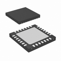
LMH6526SPX/NOPB National Semiconductor, LMH6526SPX/NOPB Datasheet - Page 13

LMH6526SPX/NOPB
Manufacturer Part Number
LMH6526SPX/NOPB
Description
IC LASER DRIVER 4CHAN 5.5V 28LLP
Manufacturer
National Semiconductor
Series
LMH™r
Type
Laser Diode Driver (CD/DVD)r
Datasheet
1.LMH6525SPNOPB.pdf
(15 pages)
Specifications of LMH6526SPX/NOPB
Number Of Channels
4
Voltage - Supply
4.5 V ~ 5.5 V
Current - Supply
33mA
Operating Temperature
-40°C ~ 85°C
Package / Case
28-LLP
Mounting Type
Surface Mount
Lead Free Status / RoHS Status
Lead free / RoHS Compliant
Other names
LMH6526SPX
Application Hints
thickness (d) en r (see Figure 2). When Checked under a
microscope: the thickness of the wires is 0.3 mm. The pitch
is 0.5 mm, while the ;r must be 1 for air. The impedance of
two parallel wires is given by this formula,
With the data above filled in this formula the result is:
Both the measured and the calculated numbers matches
very closely. The impedance of the flex cable is a physical
parameter so when designing a transmission path using this
flex cable, the impedance of the total path must be based on
140Ω. There is another parameter which is the termination
resistance inside the LMH6525 or LMH6526 which is 100Ω.
When terminating the 140Ω transmission path with an im-
pedance of 100Ω a mismatch will occur causing reflections
on the transmission line. To solve this problem it is possible
to connect directly at the input terminals of the part two
resistors of 20Ω one on every pin to keep it symmetrical.
Normally this causes signal loss over the total extra series
resistance of 40Ω when using a voltage source for driving
the transmission line. An advantage of a LVDS source is it’s
current nature. The current of a LVDS output is 3.5 mA and
this current produces across a resistor of 140Ω a voltage of
490 mV, while this voltage across the 100Ω internal termina-
tion resistor of the part remains at 350 mV, which is conform
the LVDS standard. With the usage of a series resistance of
40Ω and the termination resistor of 100Ω the total termina-
tion resistance now matches the line impedance and reflec-
tions will be as low as possible. A helpful tool for calculating
impedances of transmission lines is the: ‘Transmission Line
Rapidesigner’ available from the National Semiconductor
Interface Products Group. Application Note AN-905 details
the use of this handy software tool.
The Read Enable and Enable inputs are slower and much
less critical. The Oscillator Enable input is toggled in combi-
nation with the write pulse so special attention should be
given to this signal to insure it is routed cleanly. It may be
desirable to put a termination resistor close to the LMH6526
for the Enable Oscillator line, to achieve the best turn-on and
turn-off performance of the oscillator.
OUTPUTS
In order to achieve the fastest output rise times the layout of
the output lines should be short and tight (see Figure 3). It is
intended that the Output B trace be routed under the decou-
pling capacitor and that the ground return for the laser be
closely coupled to the output and terminated at the ground
side of the decoupling capacitor.
FIGURE 2. Parallel Wires
Z = (276/r) * log{(2*a)/d}
Z = 144Ω
(Continued)
20110122
13
The capacitance on the output lines should also be reduced
as much as possible. As always the loop area of the laser
current should be minimized and keep in mind that it is
important not to have vias in the current path of the output
lines. Via’s will introduce some inductance which lead to
extra overshoot on the pulse shape.
DECOUPLING CAPACITORS
As mentioned before, the decoupling capacitors are critical
to the performance of the part. The output section above
mentioned that the power-side decoupling capacitor should
be as close as possible to the V
the B output should pass under the decoupling capacitor.
Similarly the analog-side decoupling capacitor should be as
close as possible to the V
shows a layout where the analog (V
pling cap C1 is placed next to pins 6 and 7. (Note the layout
is rotated 90 degrees from the last figure.) The ground
extends into a plane that should connect to the oscillator
amplitude and current setting resistors. C2 is the power-side
decoupling capacitor and it can be seen placed as close to
the V
output trace. This layout has also provided for a second
power decoupling capacitor C3 that connects from V
different GND copper pour. It must be noted that the two
ground planes extending from C2 and C3 must be tied
together. This will be shown in the thermal section below.
Bear in mind that the closeness of the parts to the LMH6525/
6526 may be dictated by manufacturing rework consider-
ations such that the LMH6525/6526 can be de-soldered with
a hot-air rework station without the need to remove the
capacitors. The relevant manufacturing organization can
provide guidelines for this minimum spacing.
DD
and GNDB pins as possible while straddling the B
FIGURE 3. Laser Connection
DD
A and GNDA pins. Figure 4
DD
DD
and GND pins and that
A and GNDA) decou-
www.national.com
20110119
DD
to a


