LM2753SD/NOPB National Semiconductor, LM2753SD/NOPB Datasheet
LM2753SD/NOPB
Specifications of LM2753SD/NOPB
LM2753SDTR


Related parts for LM2753SD/NOPB

LM2753SD/NOPB Summary of contents
Page 1
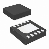
... LM2753 is available in a 10-pin No Pullback Leadless Lead- frame Package: LLP-10. Typical Application Circuit Connection Diagram © 2007 National Semiconductor Corporation Features ■ Input Voltage Range: 3.0V to 5.5V ■ Regulated 5V Output ■ ...
Page 2
Pin Descriptions Pin # Name FLASH 5 GND GND 8 I OUT 9 V OUT 10 GND Ordering Information Output Voltage Ordering Number 5.0V LM2753SD 5.0V LM2753SDX ...
Page 3
... Absolute Maximum Ratings If Military/Aerospace specified devices are required, please contact the National Semiconductor Sales Office/ Distributors for availability and specifications. If Military/Aerospace specified devices are required, please contact the National semiconductor Sales/Office/Distributors for availability and specifications. V Pin: Voltage to Ground IN EN, Flash pins: Voltage to GND ...
Page 4
Note 5: In applications where high power dissipation and/or poor package thermal resistance is present, the maximum ambient temperature may have to be derated. Maximum ambient temperature (T A-MAX dissipation of the device in the application (P - (θ following ...
Page 5
Typical Performance Characteristics GND, V(EN 10.0µ OUT Quiescent Current vs. Input Voltage Oscillator Frequency vs. Input Voltage Start-up Behavior V = 3.6V, Load = 100mA IN Top Scale: ...
Page 6
Flash Pulse Response V = 3.6V, Load = 10mA - 400mA Step IN Top Scale: 1V/Div FLASH Middle Scale: 1V/Div IOUT Bottom Scale: 100mA/Div IOUT Time scale: 100ms/Div Output Voltage Ripple vs. Input Voltage ...
Page 7
Application Information CIRCUIT DESCRIPTION The LM2753 is a Switched Capacitor Doubler with a regulated 5V output capable of continuously supplying up to 200mA load connected This device uses Pulse OUT Frequency ...
Page 8
When the output voltage is above the target reg- ulation voltage the part idles, consuming minimal supply cur- rent with C is connected between V 1 disconnected ...
Page 9
LM2753 has a switch array with multiple switches con- nected in parallel. The number of switches used in parallel depends on the input voltage applied to the LM2753. At lower input voltages all paralleled switches are used, and as ...
Page 10
Physical Dimensions www.national.com inches (millimeters) unless otherwise noted 10-Pin LLP NS Package Number SDA10A 10 ...
Page 11
Notes 11 www.national.com ...
Page 12
... National Semiconductor and the National Semiconductor logo are registered trademarks of National Semiconductor Corporation. All other brand or product names may be trademarks or registered trademarks of their respective holders. ...